TP0610T-G
RoHS  RoHS compliant
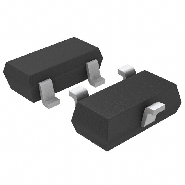
Package TO-236-3, SC-59, SOT-23-3
Category Discrete Semiconductor Products / Transistors - FETs, MOSFETs - Single
Description
Trans MOSFET P-CH 60V 0.12A 3-Pin SOT-23
PDF
/
Buying Options
Total Price: USD $0.81
Unit Price: USD $0.8096
≥1 USD $0.8096
≥10 USD $0.6776
≥100 USD $0.6248
Inventory: 1457
Minimum: 1
-
+

Technical Details
Compliance
RoHS Status ROHS3 Compliant
Radiation Hardening No
Dimensions
Width 1.3mm
Length 2.92mm
Height 930μm
Technical
Drain to Source Breakdown Voltage -60V
Gate to Source Voltage (Vgs) 20V
Continuous Drain Current (ID) 120mA
Turn-Off Delay Time 15 ns
Fall Time (Typ) 15 ns
Vgs (Max) ±20V
Drive Voltage (Max Rds On,Min Rds On) 4.5V 10V
Drain to Source Voltage (Vdss) 60V
Rise Time 15 ns
Current - Continuous Drain (Id) @ 25°C 120mA Tj
Input Capacitance (Ciss) (Max) @ Vds 60pF @ 25V
Vgs(th) (Max) @ Id 2.4V @ 1mA
Rds On (Max) @ Id, Vgs 10 Ω @ 200mA, 10V
Transistor Application SWITCHING
FET Type P-Channel
Turn On Delay Time 10 ns
Power Dissipation 360mW
Operating Mode ENHANCEMENT MODE
Element Configuration Single
Power Dissipation-Max 360mW Ta
Number of Channels 1
Number of Elements 1
Time@Peak Reflow Temperature-Max (s) 40
Peak Reflow Temperature (Cel) 260
Terminal Form GULL WING
Terminal Position DUAL
Technology MOSFET (Metal Oxide)
Subcategory Other Transistors
Additional Feature LOW THRESHOLD
ECCN Code EAR99
Number of Terminations 3
Moisture Sensitivity Level (MSL) 1 (Unlimited)
Part Status Active
JESD-609 Code e3
Published 2009
Packaging Tape & Reel (TR)
Operating Temperature -55°C~150°C TJ
Physical
Transistor Element Material SILICON
Weight 1.437803g
Number of Pins 3
Package / Case TO-236-3, SC-59, SOT-23-3
Mounting Type Surface Mount
Mount Surface Mount
Contact Plating Tin
Supply Chain
Factory Lead Time 15 Weeks
Alternative Model

Recommended For You

TP0610T-G+price,TP0610T-G+datasheet,TP0610T-G+in stock,buy+TP0610T-G,finder+TP0610T-G,TP0610T-G+tutorials,TP0610T-G+download