TP0606N3-G
RoHS  RoHS compliant
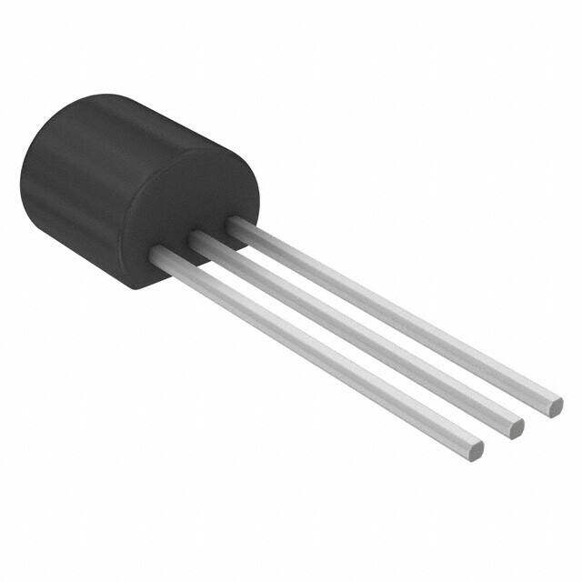
Package TO-226-3, TO-92-3 (TO-226AA)
Category Discrete Semiconductor Products / Transistors - FETs, MOSFETs - Single
Description
Trans MOSFET P-CH 60V 0.32A 3-Pin TO-92
PDF
/
Inventory: 1
Minimum: /
The more specific your information, the faster response you will get.
Please complete the following form with the details of your request part and
contact information to get a quote.
Quotation Consultation
Technical Details
Compliance
RoHS Status ROHS3 Compliant
Radiation Hardening No
Dimensions
Width 4.19mm
Length 5.21mm
Height 5.33mm
Technical
Drain to Source Breakdown Voltage -60V
Gate to Source Voltage (Vgs) 20V
Continuous Drain Current (ID) 320mA
Turn-Off Delay Time 20 ns
Fall Time (Typ) 15 ns
Vgs (Max) ±20V
Drive Voltage (Max Rds On,Min Rds On) 5V 10V
Drain to Source Voltage (Vdss) 60V
Rise Time 15 ns
Current - Continuous Drain (Id) @ 25°C 320mA Tj
Input Capacitance (Ciss) (Max) @ Vds 150pF @ 25V
Vgs(th) (Max) @ Id 2.4V @ 1mA
Rds On (Max) @ Id, Vgs 3.5 Ω @ 750mA, 10V
Transistor Application SWITCHING
FET Type P-Channel
Turn On Delay Time 10 ns
Power Dissipation 1W
Operating Mode ENHANCEMENT MODE
Element Configuration Single
Power Dissipation-Max 1W Tc
Number of Channels 1
Number of Elements 1
Terminal Form WIRE
Terminal Position BOTTOM
Technology MOSFET (Metal Oxide)
Subcategory Other Transistors
Additional Feature LOW THRESHOLD
Terminal Finish MATTE TIN
ECCN Code EAR99
Number of Terminations 3
Moisture Sensitivity Level (MSL) 1 (Unlimited)
Part Status Active
JESD-609 Code e3
Published 2011
Packaging Bulk
Operating Temperature -55°C~150°C TJ
Physical
Transistor Element Material SILICON
Weight 453.59237mg
Number of Pins 3
Package / Case TO-226-3, TO-92-3 (TO-226AA)
Mounting Type Through Hole
Mount Through Hole
Supply Chain
Factory Lead Time 6 Weeks
Alternative Model

Recommended For You

TP0606N3-G+price,TP0606N3-G+datasheet,TP0606N3-G+in stock,buy+TP0606N3-G,finder+TP0606N3-G,TP0606N3-G+tutorials,TP0606N3-G+download