TN2540N8-G
RoHS  RoHS compliant
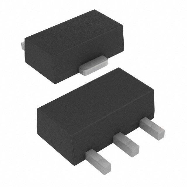
Package TO-243AA
Category Discrete Semiconductor Products / Transistors - FETs, MOSFETs - Single
Description
Trans MOSFET N-CH 400V 0.26A 4-Pin(3+Tab) SOT-89
PDF
/
Buying Options
Total Price: USD $1.47
Unit Price: USD $1.4696
≥1 USD $1.4696
≥10 USD $1.2144
≥100 USD $1.1176
Inventory: 342
Minimum: 1
-
+

Technical Details
Compliance
RoHS Status ROHS3 Compliant
Dimensions
Width 2.6mm
Length 4.6mm
Height 1.6mm
Technical
Drain to Source Breakdown Voltage 400V
Drain Current-Max (Abs) (ID) 0.57A
Gate to Source Voltage (Vgs) 20V
Continuous Drain Current (ID) 260mA
Turn-Off Delay Time 25 ns
Fall Time (Typ) 15 ns
Vgs (Max) ±20V
Drive Voltage (Max Rds On,Min Rds On) 4.5V 10V
Rise Time 15 ns
Current - Continuous Drain (Id) @ 25°C 260mA Tj
Input Capacitance (Ciss) (Max) @ Vds 125pF @ 25V
Vgs(th) (Max) @ Id 2V @ 1mA
Rds On (Max) @ Id, Vgs 12 Ω @ 500mA, 10V
Transistor Application SWITCHING
FET Type N-Channel
Turn On Delay Time 20 ns
Case Connection DRAIN
Power Dissipation 1.6W
Operating Mode ENHANCEMENT MODE
Element Configuration Single
Power Dissipation-Max 1.6W Ta
Number of Channels 1
Number of Elements 1
Qualification Status Not Qualified
JESD-30 Code R-PSSO-F3
Time@Peak Reflow Temperature-Max (s) 40
Peak Reflow Temperature (Cel) 260
Terminal Form FLAT
Technology MOSFET (Metal Oxide)
Subcategory FET General Purpose Power
Additional Feature LOW THRESHOLD
ECCN Code EAR99
Number of Terminations 3
Moisture Sensitivity Level (MSL) 1 (Unlimited)
Part Status Active
JESD-609 Code e3
Published 2013
Packaging Tape & Reel (TR)
Operating Temperature -55°C~150°C TJ
Physical
Transistor Element Material SILICON
Weight 52.786812mg
Number of Pins 4
Package / Case TO-243AA
Mounting Type Surface Mount
Mount Surface Mount
Contact Plating Tin
Supply Chain
Factory Lead Time 2 Weeks
Alternative Model

Recommended For You

TN2540N8-G+price,TN2540N8-G+datasheet,TN2540N8-G+in stock,buy+TN2540N8-G,finder+TN2540N8-G,TN2540N8-G+tutorials,TN2540N8-G+download