LND01K1-G
RoHS  RoHS compliant
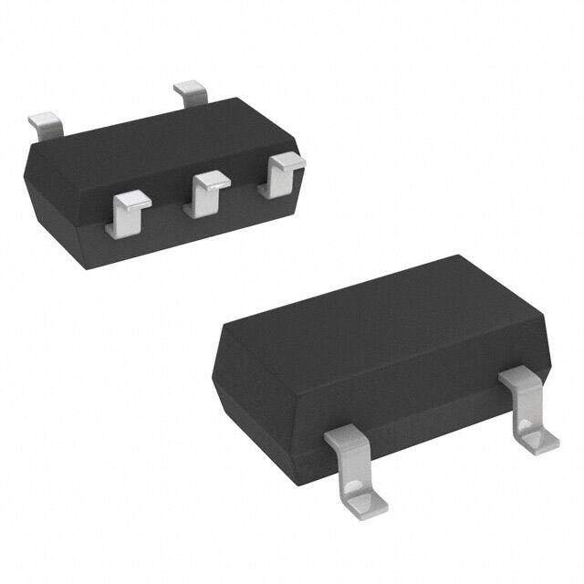
Package SC-74A, SOT-753
Category Discrete Semiconductor Products / Transistors - FETs, MOSFETs - Single
Description
MOSFET N-CH 9V 330MA SOT23-5
PDF
/
Buying Options
Total Price: USD $0.49
Unit Price: USD $0.4928
≥1 USD $0.4928
≥10 USD $0.4224
≥100 USD $0.3784
Inventory: 2496
Minimum: 1
-
+

Technical Details
Compliance
Lead Free Lead Free
RoHS Status ROHS3 Compliant
Technical
FET Feature Depletion Mode
Drain to Source Breakdown Voltage 9V
Drain Current-Max (Abs) (ID) 0.33A
Gate to Source Voltage (Vgs) 600mV
Continuous Drain Current (ID) 330mA
Turn-Off Delay Time 1 ns
Fall Time (Typ) 6.4 ns
Vgs (Max) +0.6V, -12V
Drive Voltage (Max Rds On,Min Rds On) 0V
Rise Time 11ns
Current - Continuous Drain (Id) @ 25°C 330mA Tj
Input Capacitance (Ciss) (Max) @ Vds 46pF @ 5V
Rds On (Max) @ Id, Vgs 1.4 Ω @ 100mA, 0V
Transistor Application SWITCHING
FET Type N-Channel
Turn On Delay Time 3.8 ns
Power Dissipation 360mW
Element Configuration Single
Power Dissipation-Max 360mW Ta
Number of Channels 1
Number of Elements 1
Time@Peak Reflow Temperature-Max (s) 40
Peak Reflow Temperature (Cel) 260
Terminal Form GULL WING
Terminal Position DUAL
Technology MOSFET (Metal Oxide)
Subcategory FET General Purpose Power
Terminal Finish Matte Tin (Sn)
ECCN Code EAR99
Number of Terminations 5
Moisture Sensitivity Level (MSL) 1 (Unlimited)
Part Status Active
JESD-609 Code e3
Published 2014
Packaging Tape & Reel (TR)
Operating Temperature -25°C~125°C TJ
Physical
Transistor Element Material SILICON
Weight 29.993795mg
Number of Pins 5
Package / Case SC-74A, SOT-753
Mounting Type Surface Mount
Mount Surface Mount
Supply Chain
Factory Lead Time 6 Weeks
Alternative Model

Recommended For You

LND01K1-G+price,LND01K1-G+datasheet,LND01K1-G+in stock,buy+LND01K1-G,finder+LND01K1-G,LND01K1-G+tutorials,LND01K1-G+download