IXTH75N10
RoHS  RoHS compliant
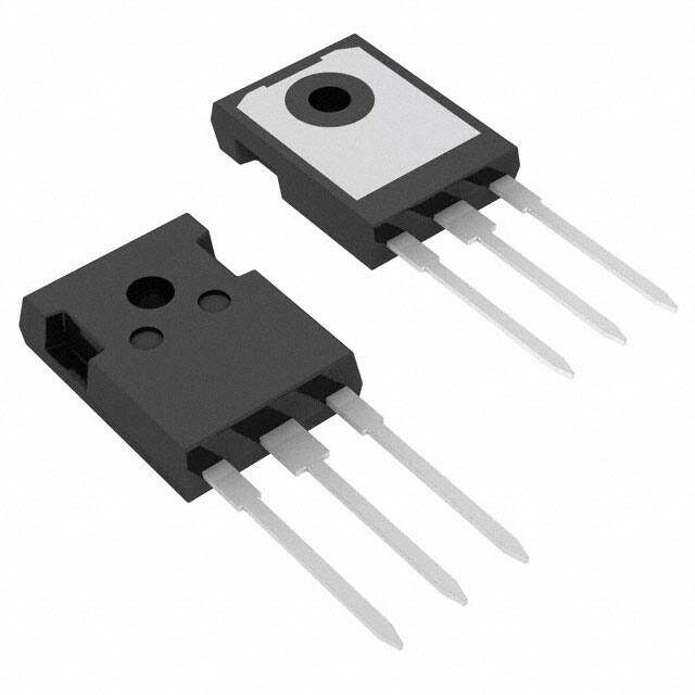
Package TO-247-3
Category Discrete Semiconductor Products / Transistors - FETs, MOSFETs - Single
Description
MOSFET N-CH 100V 75A TO247AD
PDF
/
Buying Options
Total Price: USD $4.89
Unit Price: USD $4.891918
≥1 USD $4.891918
≥10 USD $4.615019
≥100 USD $4.353785
≥500 USD $4.107351
≥1000 USD $3.874855
Inventory: 1181
Minimum: 1
-
+

Technical Details
Compliance
Lead Free Lead Free
RoHS Status ROHS3 Compliant
REACH SVHC No SVHC
Radiation Hardening No
Technical
Nominal Vgs 4 V
Dual Supply Voltage 100V
Drain to Source Breakdown Voltage 100V
Gate to Source Voltage (Vgs) 20V
JEDEC-95 Code TO-247AD
Threshold Voltage 4V
Continuous Drain Current (ID) 75A
Turn-Off Delay Time 100 ns
Fall Time (Typ) 30 ns
Vgs (Max) ±20V
Drive Voltage (Max Rds On,Min Rds On) 10V
Rise Time 60ns
Gate Charge (Qg) (Max) @ Vgs 260nC @ 10V
Current - Continuous Drain (Id) @ 25°C 75A Tc
Input Capacitance (Ciss) (Max) @ Vds 4500pF @ 25V
Vgs(th) (Max) @ Id 4V @ 4mA
Rds On (Max) @ Id, Vgs 20m Ω @ 37.5A, 10V
Transistor Application SWITCHING
FET Type N-Channel
Case Connection DRAIN
Power Dissipation 300W
Operating Mode ENHANCEMENT MODE
Element Configuration Single
Power Dissipation-Max 300W Tc
Number of Elements 1
Pin Count 3
Current Rating 75A
Technology MOSFET (Metal Oxide)
Voltage - Rated DC 100V
Subcategory FET General Purpose Power
Resistance 20mOhm
ECCN Code EAR99
Number of Terminations 3
Moisture Sensitivity Level (MSL) Not Applicable
Part Status Not For New Designs
Pbfree Code yes
Series MegaMOS?
Published 2003
Packaging Tube
Operating Temperature -55°C~150°C TJ
Physical
Transistor Element Material SILICON
Number of Pins 3
Package / Case TO-247-3
Mounting Type Through Hole
Mount Through Hole
Supply Chain
Factory Lead Time 8 Weeks
Alternative Model

Recommended For You

IXTH75N10+price,IXTH75N10+datasheet,IXTH75N10+in stock,buy+IXTH75N10,finder+IXTH75N10,IXTH75N10+tutorials,IXTH75N10+download