IXTH5N100A
RoHS  RoHS compliant
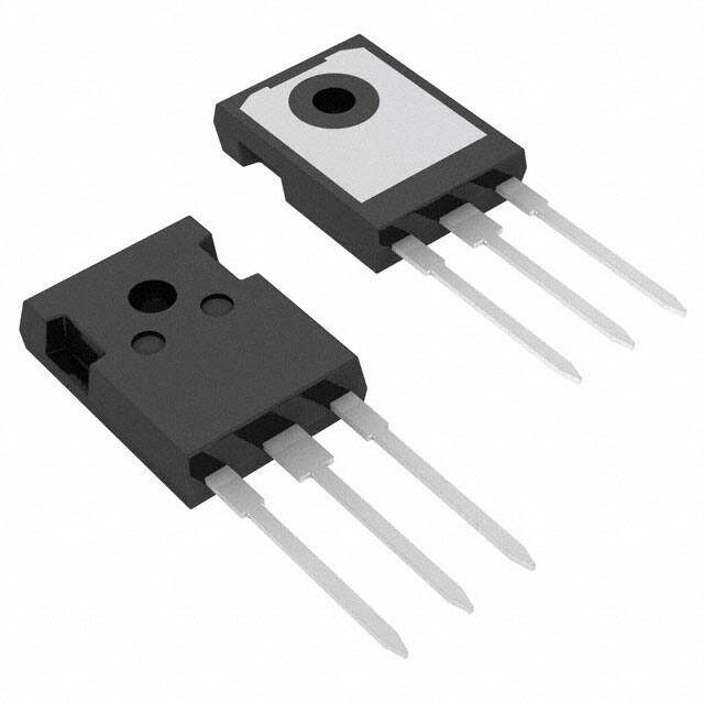
Package TO-247-3
Category Discrete Semiconductor Products / Transistors - FETs, MOSFETs - Single
Description
MOSFET N-CH 1000V 5A TO247AD
PDF
/
Inventory: 9108
Minimum: /
The more specific your information, the faster response you will get.
Please complete the following form with the details of your request part and
contact information to get a quote.
Quotation Consultation
Technical Details
Compliance
Lead Free Lead Free
RoHS Status ROHS3 Compliant
Radiation Hardening No
Technical
Pulsed Drain Current-Max (IDM) 20A
Drain to Source Breakdown Voltage 1kV
Drain Current-Max (Abs) (ID) 5A
Gate to Source Voltage (Vgs) 20V
JEDEC-95 Code TO-247AD
Continuous Drain Current (ID) 5A
Turn-Off Delay Time 100 ns
Fall Time (Typ) 30 ns
Vgs (Max) ±20V
Drive Voltage (Max Rds On,Min Rds On) 10V
Drain to Source Voltage (Vdss) 1000V
Rise Time 20ns
Gate Charge (Qg) (Max) @ Vgs 130nC @ 10V
Current - Continuous Drain (Id) @ 25°C 5A Tc
Input Capacitance (Ciss) (Max) @ Vds 2600pF @ 25V
Vgs(th) (Max) @ Id 4.5V @ 250μA
Rds On (Max) @ Id, Vgs 2 Ω @ 2.5A, 10V
Transistor Application SWITCHING
FET Type N-Channel
Case Connection DRAIN
Power Dissipation 180W
Operating Mode ENHANCEMENT MODE
Element Configuration Single
Power Dissipation-Max 180W Tc
Number of Elements 1
Pin Count 3
Current Rating 5A
Technology MOSFET (Metal Oxide)
Voltage - Rated DC 1kV
Subcategory FET General Purpose Power
Resistance 2.4Ohm
Number of Terminations 3
Part Status Active
Pbfree Code yes
Published 2000
Packaging Tube
Operating Temperature -55°C~150°C TJ
Physical
Transistor Element Material SILICON
Number of Pins 3
Package / Case TO-247-3
Mounting Type Through Hole
Mount Through Hole
Supply Chain
Factory Lead Time 28 Weeks
Alternative Model

Recommended For You

IXTH5N100A+price,IXTH5N100A+datasheet,IXTH5N100A+in stock,buy+IXTH5N100A,finder+IXTH5N100A,IXTH5N100A+tutorials,IXTH5N100A+download