IXFT14N100
RoHS
/
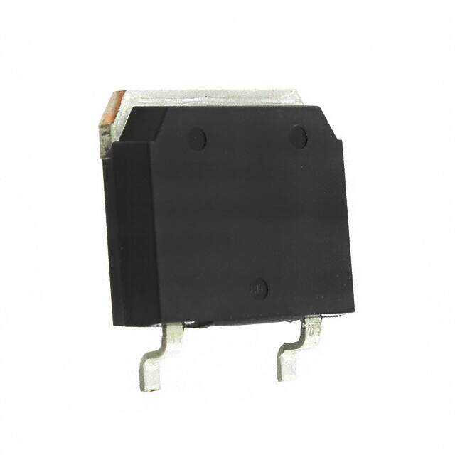
Package TO-268-3, D3Pak (2 Leads + Tab), TO-268AA
Category Discrete Semiconductor Products / Transistors - FETs, MOSFETs - Single
Description
Trans MOSFET N-CH 1KV 14A 3-Pin(2+Tab) TO-268
PDF
/
Inventory: 6686
Minimum: /
The more specific your information, the faster response you will get.
Please complete the following form with the details of your request part and
contact information to get a quote.
Quotation Consultation
Technical Details
Compliance
RoHS Status RoHS Compliant
Technical
Pulsed Drain Current-Max (IDM) 56A
Drain to Source Breakdown Voltage 1kV
Drain-source On Resistance-Max 0.75Ohm
Gate to Source Voltage (Vgs) 20V
Continuous Drain Current (ID) 14A
Turn-Off Delay Time 120 ns
Fall Time (Typ) 30 ns
Vgs (Max) ±20V
Drive Voltage (Max Rds On,Min Rds On) 10V
Drain to Source Voltage (Vdss) 1000V
Rise Time 30ns
Gate Charge (Qg) (Max) @ Vgs 220nC @ 10V
Current - Continuous Drain (Id) @ 25°C 14A Tc
Input Capacitance (Ciss) (Max) @ Vds 4500pF @ 25V
Vgs(th) (Max) @ Id 4.5V @ 4mA
Rds On (Max) @ Id, Vgs 750m Ω @ 500mA, 10V
Transistor Application SWITCHING
FET Type N-Channel
Case Connection DRAIN
Power Dissipation 360W
Operating Mode ENHANCEMENT MODE
Element Configuration Single
Power Dissipation-Max 360W Tc
Number of Elements 1
Qualification Status Not Qualified
JESD-30 Code R-PSSO-G2
Pin Count 4
Time@Peak Reflow Temperature-Max (s) NOT SPECIFIED
Peak Reflow Temperature (Cel) NOT SPECIFIED
Terminal Form GULL WING
Technology MOSFET (Metal Oxide)
Subcategory FET General Purpose Power
Additional Feature AVALANCHE RATED
Terminal Finish Matte Tin (Sn)
Number of Terminations 2
Moisture Sensitivity Level (MSL) 1 (Unlimited)
Part Status Obsolete
Pbfree Code yes
JESD-609 Code e3
Series HiPerFET?
Published 2000
Packaging Tube
Operating Temperature -55°C~150°C TJ
Physical
Transistor Element Material SILICON
Package / Case TO-268-3, D3Pak (2 Leads + Tab), TO-268AA
Mounting Type Surface Mount
Mount Surface Mount
Alternative Model

Recommended For You

IXFT14N100+price,IXFT14N100+datasheet,IXFT14N100+in stock,buy+IXFT14N100,finder+IXFT14N100,IXFT14N100+tutorials,IXFT14N100+download