SPN03N60C3
RoHS
/
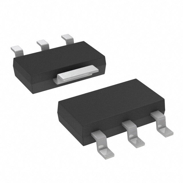
Package TO-261-4, TO-261AA
Category Discrete Semiconductor Products / Transistors - FETs, MOSFETs - Single
Description
MOSFET N-CH 650V 0.7A SOT-223
PDF
/
Buying Options
Total Price: USD $0.3
Unit Price: USD $0.30495
≥1 USD $0.30495
≥10 USD $0.24985
≥100 USD $0.24225
≥500 USD $0.23465
≥1000 USD $0.22705
Inventory: 1237
Minimum: 1
-
+

Technical Details
Compliance
Lead Free Contains Lead
RoHS Status Non-RoHS Compliant
Technical
Nominal Vgs 3 V
Pulsed Drain Current-Max (IDM) 3A
Drain to Source Breakdown Voltage 650V
Drain Current-Max (Abs) (ID) 0.7A
Gate to Source Voltage (Vgs) 20V
Continuous Drain Current (ID) 700mA
Turn-Off Delay Time 64 ns
Fall Time (Typ) 3 ns
Vgs (Max) ±20V
Drive Voltage (Max Rds On,Min Rds On) 10V
Rise Time 3ns
Gate Charge (Qg) (Max) @ Vgs 17nC @ 10V
Current - Continuous Drain (Id) @ 25°C 700mA Ta
Input Capacitance (Ciss) (Max) @ Vds 400pF @ 25V
Vgs(th) (Max) @ Id 3.9V @ 135μA
Rds On (Max) @ Id, Vgs 1.4 Ω @ 2A, 10V
Transistor Application SWITCHING
FET Type N-Channel
Case Connection DRAIN
Power Dissipation 1.8W
Operating Mode ENHANCEMENT MODE
Power Dissipation-Max 1.8W Ta
Configuration SINGLE WITH BUILT-IN DIODE
Number of Elements 1
Qualification Status Not Qualified
JESD-30 Code R-PDSO-G4
Pin Count 4
Time@Peak Reflow Temperature-Max (s) NOT SPECIFIED
Current Rating 700mA
Peak Reflow Temperature (Cel) NOT SPECIFIED
Terminal Form GULL WING
Terminal Position DUAL
Technology MOSFET (Metal Oxide)
Voltage - Rated DC 650V
Subcategory FET General Purpose Power
HTS Code 8541.29.00.95
Terminal Finish Tin/Lead (Sn/Pb)
ECCN Code EAR99
Number of Terminations 4
Moisture Sensitivity Level (MSL) 1 (Unlimited)
Part Status Obsolete
JESD-609 Code e0
Series CoolMOS?
Published 2004
Packaging Tape & Reel (TR)
Operating Temperature -55°C~150°C TJ
Physical
Transistor Element Material SILICON
Number of Pins 3
Package / Case TO-261-4, TO-261AA
Mounting Type Surface Mount
Mount Surface Mount
Alternative Model

Recommended For You

SPN03N60C3+price,SPN03N60C3+datasheet,SPN03N60C3+in stock,buy+SPN03N60C3,finder+SPN03N60C3,SPN03N60C3+tutorials,SPN03N60C3+download