IRLS4030PBF
RoHS  RoHS compliant
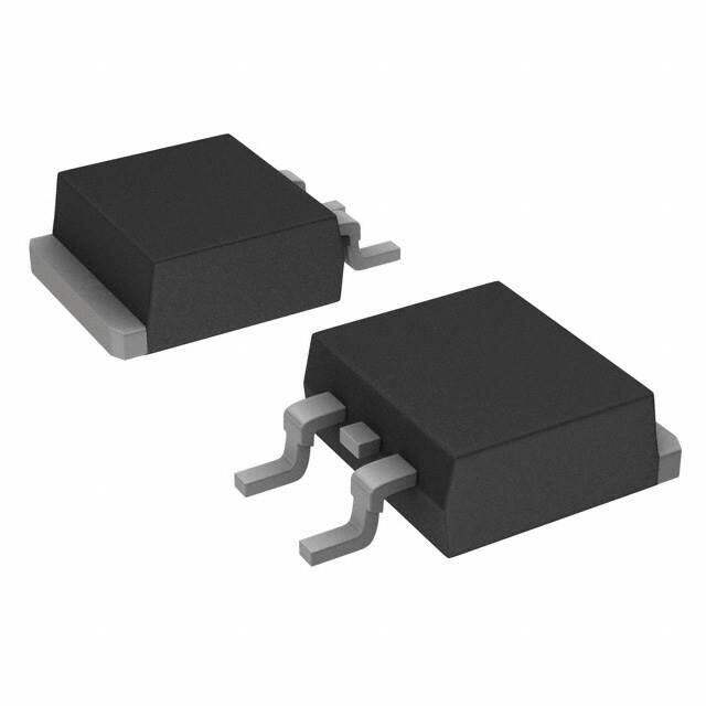
Package TO-263-3, D2Pak (2 Leads + Tab), TO-263AB
Category Discrete Semiconductor Products / Transistors - FETs, MOSFETs - Single
Description
MOSFET N-CH 100V 180A D2PAK
PDF
/
Buying Options
Total Price: USD $4.15
Unit Price: USD $4.1477
≥1 USD $4.1477
≥10 USD $3.40385
≥100 USD $3.29745
≥500 USD $3.19105
≥1000 USD $3.08465
Inventory: 1155
Minimum: 1
-
+

Technical Details
Technical
Vgs(th) (Max) @ Id 2.5V @ 250μA
Input Capacitance (Ciss) (Max) @ Vds 11360pF @ 50V
Current - Continuous Drain (Id) @ 25°C 180A Tc
Gate Charge (Qg) (Max) @ Vgs 130nC @ 4.5V
Rise Time 330 ns
Drive Voltage (Max Rds On,Min Rds On) 4.5V 10V
Vgs (Max) ±16V
Fall Time (Typ) 170 ns
Turn-Off Delay Time 110 ns
Continuous Drain Current (ID) 190A
Threshold Voltage 2.5V
Gate to Source Voltage (Vgs) 16V
Drain to Source Breakdown Voltage 100V
Dual Supply Voltage 100V
Nominal Vgs 2.5 V
Rds On (Max) @ Id, Vgs 4.3m Ω @ 110A, 10V
Transistor Application SWITCHING
FET Type N-Channel
Turn On Delay Time 74 ns
Power Dissipation 370W
Operating Mode ENHANCEMENT MODE
Element Configuration Single
Power Dissipation-Max 370W Tc
Number of Elements 1
JESD-30 Code R-PSSO-G2
Time@Peak Reflow Temperature-Max (s) 30
Peak Reflow Temperature (Cel) 260
Terminal Form GULL WING
Technology MOSFET (Metal Oxide)
Subcategory FET General Purpose Power
Terminal Finish Matte Tin (Sn) - with Nickel (Ni) barrier
Resistance 4.3MOhm
ECCN Code EAR99
Termination SMD/SMT
Number of Terminations 2
Moisture Sensitivity Level (MSL) 1 (Unlimited)
Part Status Discontinued
JESD-609 Code e3
Series HEXFET?
Published 2009
Packaging Tube
Operating Temperature -55°C~175°C TJ
Dimensions
Height 4.572mm
Length 10.668mm
Width 9.65mm
Compliance
Radiation Hardening No
Lead Free Lead Free
RoHS Status ROHS3 Compliant
REACH SVHC No SVHC
Physical
Transistor Element Material SILICON
Number of Pins 3
Package / Case TO-263-3, D2Pak (2 Leads + Tab), TO-263AB
Mounting Type Surface Mount
Mount Surface Mount
Alternative Model

Recommended For You

IRLS4030PBF+price,IRLS4030PBF+datasheet,IRLS4030PBF+in stock,buy+IRLS4030PBF,finder+IRLS4030PBF,IRLS4030PBF+tutorials,IRLS4030PBF+download