IRLL014NTRPBF
RoHS  RoHS compliant
Package TO-261-4, TO-261AA
Category Discrete Semiconductor Products / Transistors - FETs, MOSFETs - Single
Description
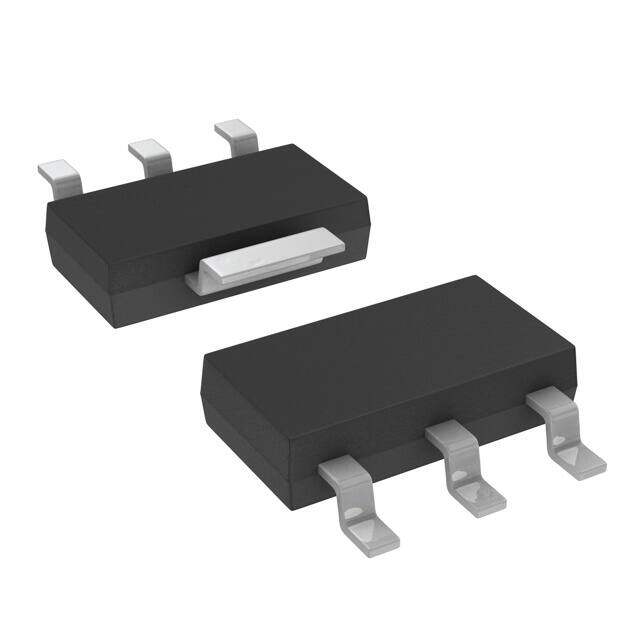
MOSFET N-CH 55V 2A SOT223
PDF
/
Buying Options
Total Price: USD $0.57
Unit Price: USD $0.572
≥1 USD $0.572
≥10 USD $0.49808
≥100 USD $0.344784
≥500 USD $0.288077
≥1000 USD $0.245168
Inventory: 6890
Minimum: 1
-
+

Technical Details
Compliance
Lead Free Lead Free
RoHS Status ROHS3 Compliant
REACH SVHC No SVHC
Radiation Hardening No
Dimensions
Width 3.7mm
Length 6.6802mm
Height 1.4478mm
Technical
Nominal Vgs 2 V
Recovery Time 61 ns
Dual Supply Voltage 55V
Drain to Source Breakdown Voltage 55V
Drain Current-Max (Abs) (ID) 2A
Gate to Source Voltage (Vgs) 16V
Threshold Voltage 2V
Continuous Drain Current (ID) 2A
Turn-Off Delay Time 14 ns
Fall Time (Typ) 2.9 ns
Vgs (Max) ±16V
Drive Voltage (Max Rds On,Min Rds On) 4V 10V
Rise Time 4.9 ns
Gate Charge (Qg) (Max) @ Vgs 14nC @ 10V
Current - Continuous Drain (Id) @ 25°C 2A Ta
Input Capacitance (Ciss) (Max) @ Vds 230pF @ 25V
Vgs(th) (Max) @ Id 2V @ 250μA
Rds On (Max) @ Id, Vgs 140m Ω @ 2A, 10V
Transistor Application SWITCHING
FET Type N-Channel
Turn On Delay Time 5.1 ns
Case Connection DRAIN
Power Dissipation 2.1W
Operating Mode ENHANCEMENT MODE
Element Configuration Single
Power Dissipation-Max 1W Ta
Number of Elements 1
JESD-30 Code R-PDSO-G4
Current Rating 2A
Terminal Form GULL WING
Terminal Position DUAL
Technology MOSFET (Metal Oxide)
Voltage - Rated DC 55V
Additional Feature AVALANCHE RATED, ULTRA LOW RESISTANCE
Resistance 200mOhm
ECCN Code EAR99
Number of Terminations 4
Moisture Sensitivity Level (MSL) 1 (Unlimited)
Part Status Active
JESD-609 Code e3
Series HEXFET?
Published 1999
Packaging Tape & Reel (TR)
Operating Temperature -55°C~150°C TJ
Physical
Transistor Element Material SILICON
Number of Pins 3
Package / Case TO-261-4, TO-261AA
Mounting Type Surface Mount
Mount Surface Mount
Contact Plating Tin
Supply Chain
Factory Lead Time 12 Weeks
Alternative Model

Recommended For You
IRLL014NTRPBF+price,IRLL014NTRPBF+datasheet,IRLL014NTRPBF+in stock,buy+IRLL014NTRPBF,finder+IRLL014NTRPBF,IRLL014NTRPBF+tutorials,IRLL014NTRPBF+download