IRFS4010TRL7PP
RoHS  RoHS compliant
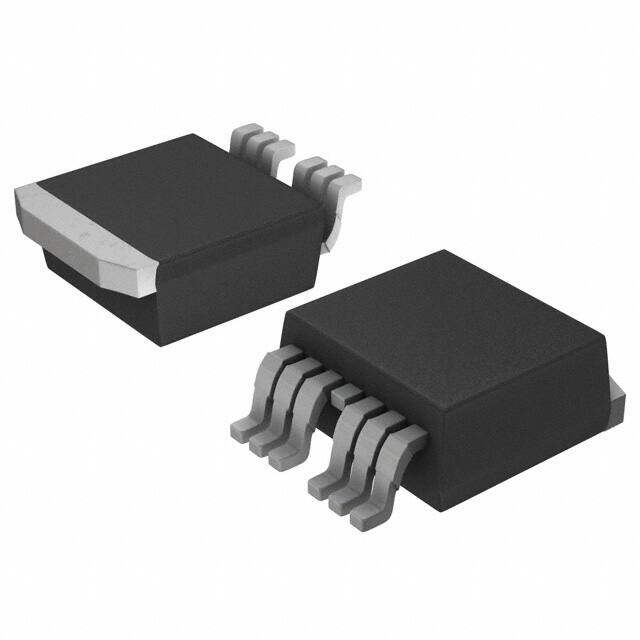
Package TO-263-7, D2Pak (6 Leads + Tab), TO-263CB
Category Discrete Semiconductor Products / Transistors - FETs, MOSFETs - Single
Description
MOSFET N-CH 100V 190A D2PAK-7
PDF
/
Buying Options
Total Price: USD $4.37
Unit Price: USD $4.3736
≥1 USD $4.3736
≥10 USD $3.67488
≥100 USD $2.972816
Inventory: 1151
Minimum: 1
-
+

Technical Details
Compliance
Lead Free Lead Free
RoHS Status ROHS3 Compliant
REACH SVHC No SVHC
Radiation Hardening No
Technical
Nominal Vgs 4 V
Drain to Source Breakdown Voltage 100V
Gate to Source Voltage (Vgs) 20V
Continuous Drain Current (ID) 190A
Turn-Off Delay Time 100 ns
Fall Time (Typ) 48 ns
Vgs (Max) ±20V
Drive Voltage (Max Rds On,Min Rds On) 10V
Rise Time 56ns
Gate Charge (Qg) (Max) @ Vgs 230nC @ 10V
Current - Continuous Drain (Id) @ 25°C 190A Tc
Input Capacitance (Ciss) (Max) @ Vds 9830pF @ 50V
Vgs(th) (Max) @ Id 4V @ 250μA
Rds On (Max) @ Id, Vgs 4m Ω @ 110A, 10V
FET Type N-Channel
Turn On Delay Time 19 ns
Power Dissipation 380W
Operating Mode ENHANCEMENT MODE
Power Dissipation-Max 380W Tc
Configuration Single
Number of Elements 1
Technology MOSFET (Metal Oxide)
Subcategory FET General Purpose Power
Terminal Finish Matte Tin (Sn) - with Nickel (Ni) barrier
ECCN Code EAR99
Moisture Sensitivity Level (MSL) 1 (Unlimited)
Part Status Active
JESD-609 Code e3
Series HEXFET?
Published 2008
Packaging Tape & Reel (TR)
Operating Temperature -55°C~175°C TJ
Physical
Number of Pins 7
Package / Case TO-263-7, D2Pak (6 Leads + Tab), TO-263CB
Mounting Type Surface Mount
Mount Surface Mount
Supply Chain
Factory Lead Time 12 Weeks
Alternative Model

Recommended For You

IRFS4010TRL7PP+price,IRFS4010TRL7PP+datasheet,IRFS4010TRL7PP+in stock,buy+IRFS4010TRL7PP,finder+IRFS4010TRL7PP,IRFS4010TRL7PP+tutorials,IRFS4010TRL7PP+download