IRFR7746PBF
RoHS  RoHS compliant
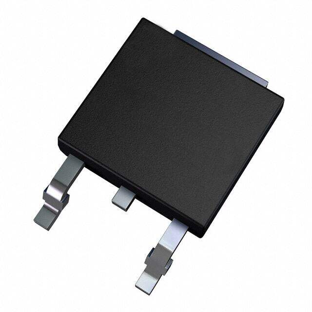
Package TO-252-3, DPak (2 Leads + Tab), SC-63
Category Discrete Semiconductor Products / Transistors - FETs, MOSFETs - Single
Description
MOSFET N-CH 75V 56A D2PAK
PDF
/
Buying Options
Total Price: USD $2.68
Unit Price: USD $2.6847
≥1 USD $2.6847
≥10 USD $2.20305
≥100 USD $2.13465
≥500 USD $2.0653
≥1000 USD $1.9969
Inventory: 339
Minimum: 1
-
+

Technical Details
Compliance
Lead Free Lead Free
RoHS Status ROHS3 Compliant
REACH SVHC No SVHC
Dimensions
Width 6.22mm
Length 6.73mm
Height 2.39mm
Technical
Gate to Source Voltage (Vgs) 20V
Threshold Voltage 3.7V
Continuous Drain Current (ID) 56A
Turn-Off Delay Time 34 ns
Fall Time (Typ) 21 ns
Vgs (Max) ±20V
Drive Voltage (Max Rds On,Min Rds On) 6V 10V
Drain to Source Voltage (Vdss) 75V
Rise Time 30ns
Gate Charge (Qg) (Max) @ Vgs 89nC @ 10V
Current - Continuous Drain (Id) @ 25°C 56A Tc
Input Capacitance (Ciss) (Max) @ Vds 3107pF @ 25V
Vgs(th) (Max) @ Id 3.7V @ 100μA
Rds On (Max) @ Id, Vgs 11.2m Ω @ 35A, 10V
FET Type N-Channel
Turn On Delay Time 7.9 ns
Element Configuration Single
Power Dissipation-Max 99W Tc
Number of Channels 1
Time@Peak Reflow Temperature-Max (s) NOT SPECIFIED
Reach Compliance Code not_compliant
Peak Reflow Temperature (Cel) NOT SPECIFIED
Technology MOSFET (Metal Oxide)
Terminal Finish Matte Tin (Sn) - with Nickel (Ni) barrier
ECCN Code EAR99
Moisture Sensitivity Level (MSL) 1 (Unlimited)
Part Status Discontinued
JESD-609 Code e3
Series HEXFET?
Published 2006
Packaging Tube
Operating Temperature -55°C~175°C TJ
Physical
Weight 3.949996g
Number of Pins 3
Package / Case TO-252-3, DPak (2 Leads + Tab), SC-63
Mounting Type Surface Mount
Mount Surface Mount, Through Hole
Alternative Model

Recommended For You

IRFR7746PBF+price,IRFR7746PBF+datasheet,IRFR7746PBF+in stock,buy+IRFR7746PBF,finder+IRFR7746PBF,IRFR7746PBF+tutorials,IRFR7746PBF+download