IRFP3703PBF
RoHS  RoHS compliant
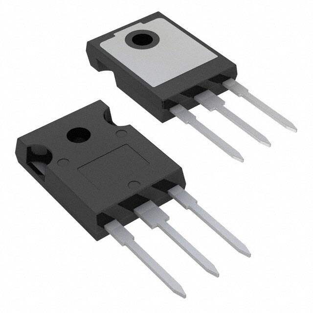
Package TO-247-3
Category Discrete Semiconductor Products / Transistors - FETs, MOSFETs - Single
Description
MOSFET N-CH 30V 210A TO-247AC
PDF
/
Buying Options
Total Price: USD $5.81
Unit Price: USD $5.8064
≥1 USD $5.8064
≥10 USD $4.76425
≥100 USD $4.61605
≥500 USD $4.4669
≥1000 USD $4.31775
Inventory: 9752
Minimum: 1
-
+

Technical Details
Compliance
Lead Free Lead Free
RoHS Status ROHS3 Compliant
REACH SVHC No SVHC
Radiation Hardening No
Dimensions
Width 5.3086mm
Length 15.87mm
Height 20.7mm
Technical
Nominal Vgs 4 V
Recovery Time 120 ns
Dual Supply Voltage 30V
Drain to Source Breakdown Voltage 30V
Drain Current-Max (Abs) (ID) 90A
Gate to Source Voltage (Vgs) 20V
JEDEC-95 Code TO-247AC
Continuous Drain Current (ID) 210A
Turn-Off Delay Time 53 ns
Fall Time (Typ) 24 ns
Vgs (Max) ±20V
Drive Voltage (Max Rds On,Min Rds On) 7V 10V
Rise Time 123 ns
Gate Charge (Qg) (Max) @ Vgs 209nC @ 10V
Current - Continuous Drain (Id) @ 25°C 210A Tc
Input Capacitance (Ciss) (Max) @ Vds 8250pF @ 25V
Vgs(th) (Max) @ Id 4V @ 250μA
Rds On (Max) @ Id, Vgs 2.8m Ω @ 76A, 10V
Transistor Application SWITCHING
FET Type N-Channel
Turn On Delay Time 18 ns
Case Connection DRAIN
Power Dissipation 230W
Operating Mode ENHANCEMENT MODE
Element Configuration Single
Power Dissipation-Max 3.8W Ta 230W Tc
Number of Elements 1
Current Rating 210A
Technology MOSFET (Metal Oxide)
Voltage - Rated DC 30V
Subcategory FET General Purpose Power
Additional Feature AVALANCHE RATED, ULTRA LOW RESISTANCE
ECCN Code EAR99
Termination Through Hole
Number of Terminations 3
Moisture Sensitivity Level (MSL) 1 (Unlimited)
Part Status Active
Series HEXFET?
Published 2001
Packaging Bulk
Operating Temperature -55°C~175°C TJ
Physical
Transistor Element Material SILICON
Number of Pins 3
Package / Case TO-247-3
Mounting Type Through Hole
Mount Through Hole
Supply Chain
Factory Lead Time 12 Weeks
Alternative Model

Recommended For You

IRFP3703PBF+price,IRFP3703PBF+datasheet,IRFP3703PBF+in stock,buy+IRFP3703PBF,finder+IRFP3703PBF,IRFP3703PBF+tutorials,IRFP3703PBF+download