IRFHS8342TRPBF
RoHS  RoHS compliant
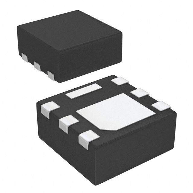
Package 6-PowerVDFN
Category Discrete Semiconductor Products / Transistors - FETs, MOSFETs - Single
Description
INFINEON IRFHS8342TRPBF MOSFET Transistor, N Channel, 8.8 A, 30 V, 0.013 ohm, 10 V, 1.8 VNew
PDF
/
Buying Options
Total Price: USD $0.44
Unit Price: USD $0.44
≥1 USD $0.44
≥10 USD $0.37312
≥100 USD $0.259512
≥500 USD $0.202611
≥1000 USD $0.164692
≥3000 USD $0.147224
Inventory: 70422
Minimum: 1
-
+

Technical Details
Compliance
Lead Free Lead Free
RoHS Status ROHS3 Compliant
REACH SVHC No SVHC
Radiation Hardening No
Technical
Nominal Vgs 1.8 V
Drain to Source Breakdown Voltage 30V
Drain Current-Max (Abs) (ID) 8.5A
Gate to Source Voltage (Vgs) 20V
Threshold Voltage 1.8V
Continuous Drain Current (ID) 8.8A
Turn-Off Delay Time 5.2 ns
Fall Time (Typ) 5 ns
Vgs (Max) ±20V
Drive Voltage (Max Rds On,Min Rds On) 4.5V 10V
Rise Time 15 ns
Gate Charge (Qg) (Max) @ Vgs 8.7nC @ 10V
Current - Continuous Drain (Id) @ 25°C 8.8A Ta 19A Tc
Input Capacitance (Ciss) (Max) @ Vds 600pF @ 25V
Vgs(th) (Max) @ Id 2.35V @ 25μA
Rds On (Max) @ Id, Vgs 16m Ω @ 8.5A, 10V
Transistor Application SWITCHING
FET Type N-Channel
Turn On Delay Time 5.9 ns
Case Connection DRAIN
Power Dissipation 2.1W
Operating Mode ENHANCEMENT MODE
Power Dissipation-Max 2.1W Ta
Configuration SINGLE WITH BUILT-IN DIODE
Number of Elements 1
Terminal Position DUAL
Technology MOSFET (Metal Oxide)
Subcategory FET General Purpose Power
Terminal Finish Matte Tin (Sn)
Resistance 16MOhm
ECCN Code EAR99
Number of Terminations 6
Moisture Sensitivity Level (MSL) 1 (Unlimited)
Part Status Active
JESD-609 Code e3
Series HEXFET?
Published 2010
Packaging Tape & Reel (TR)
Operating Temperature -55°C~150°C TJ
Physical
Transistor Element Material SILICON
Number of Pins 6
Package / Case 6-PowerVDFN
Mounting Type Surface Mount
Mount Surface Mount
Supply Chain
Factory Lead Time 12 Weeks
Alternative Model

Recommended For You

IRFHS8342TRPBF+price,IRFHS8342TRPBF+datasheet,IRFHS8342TRPBF+in stock,buy+IRFHS8342TRPBF,finder+IRFHS8342TRPBF,IRFHS8342TRPBF+tutorials,IRFHS8342TRPBF+download