IRFH5053TRPBF
RoHS  RoHS compliant
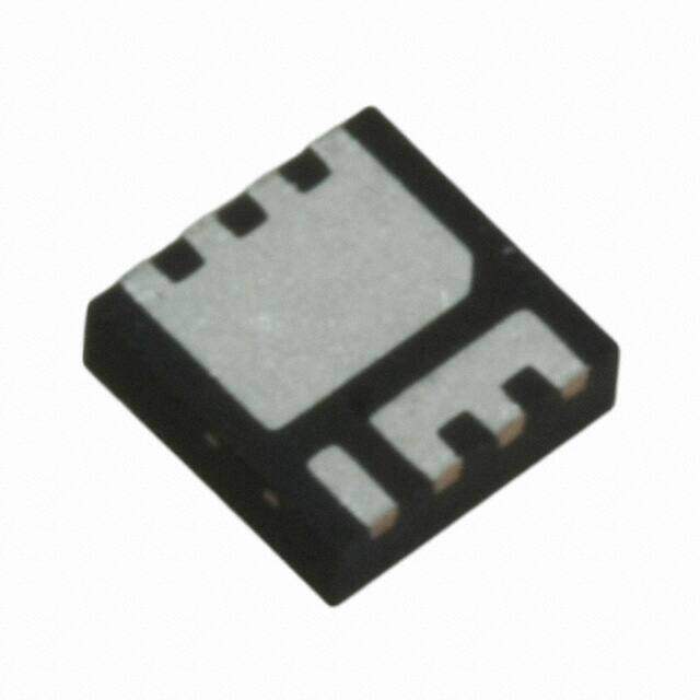
Package 8-PowerVDFN
Category Discrete Semiconductor Products / Transistors - FETs, MOSFETs - Single
Description
MOSFET N-CH 100V 9.3A PQFN56
PDF
/
Buying Options
Total Price: USD $1.87
Unit Price: USD $1.8744
≥1 USD $1.8744
≥10 USD $1.56024
≥100 USD $1.241768
≥500 USD $1.050755
≥1000 USD $0.891554
≥3000 USD $0.846982
Inventory: 1162
Minimum: 1
-
+

Technical Details
Compliance
Lead Free Lead Free
RoHS Status ROHS3 Compliant
REACH SVHC No SVHC
Dimensions
Width 5mm
Length 5.9944mm
Height 939.8μm
Technical
Nominal Vgs 3.7 V
Pulsed Drain Current-Max (IDM) 75A
Drain to Source Breakdown Voltage 100V
Drain Current-Max (Abs) (ID) 9.3A
Gate to Source Voltage (Vgs) 20V
Threshold Voltage 3.7V
Continuous Drain Current (ID) 9.3mA
Turn-Off Delay Time 18 ns
Fall Time (Typ) 9.9 ns
Vgs (Max) ±20V
Drive Voltage (Max Rds On,Min Rds On) 10V
Rise Time 14.6 ns
Gate Charge (Qg) (Max) @ Vgs 36nC @ 10V
Current - Continuous Drain (Id) @ 25°C 9.3A Ta 46A Tc
Input Capacitance (Ciss) (Max) @ Vds 1510pF @ 50V
Vgs(th) (Max) @ Id 4.9V @ 100μA
Rds On (Max) @ Id, Vgs 18m Ω @ 9.3A, 10V
Transistor Application SWITCHING
FET Type N-Channel
Turn On Delay Time 8.6 ns
Case Connection DRAIN
Power Dissipation 3.1W
Operating Mode ENHANCEMENT MODE
Power Dissipation-Max 3.1W Ta 8.3W Tc
Configuration SINGLE WITH BUILT-IN DIODE
Number of Elements 1
Qualification Status Not Qualified
JESD-30 Code R-PDSO-N3
Time@Peak Reflow Temperature-Max (s) 30
Peak Reflow Temperature (Cel) 260
Terminal Form NO LEAD
Terminal Position DUAL
Technology MOSFET (Metal Oxide)
Subcategory FET General Purpose Power
Terminal Finish Matte Tin (Sn)
ECCN Code EAR99
Number of Terminations 3
Moisture Sensitivity Level (MSL) 2 (1 Year)
Part Status Active
JESD-609 Code e3
Series HEXFET?
Published 2005
Packaging Tape & Reel (TR)
Operating Temperature -55°C~150°C TJ
Physical
Transistor Element Material SILICON
Number of Pins 8
Package / Case 8-PowerVDFN
Mounting Type Surface Mount
Mount Surface Mount
Supply Chain
Factory Lead Time 12 Weeks
Alternative Model

Recommended For You

IRFH5053TRPBF+price,IRFH5053TRPBF+datasheet,IRFH5053TRPBF+in stock,buy+IRFH5053TRPBF,finder+IRFH5053TRPBF,IRFH5053TRPBF+tutorials,IRFH5053TRPBF+download