IRFB4321PBF
RoHS  RoHS compliant
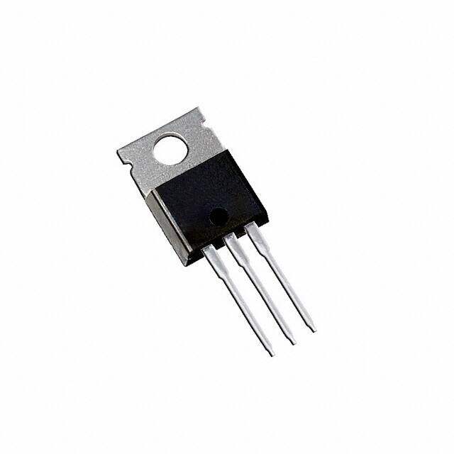
Package TO-220-3
Category Discrete Semiconductor Products / Transistors - FETs, MOSFETs - Single
Description
MOSFET N-CH 150V 83A TO-220AB
PDF
/
Buying Options
Total Price: USD $1.77
Unit Price: USD $1.76747
≥1 USD $1.76747
≥10 USD $1.66742
≥100 USD $1.57304
≥500 USD $1.484
≥1000 USD $1.4
≥3000 USD $1.32075
Inventory: 3120
Minimum: 1
-
+

Technical Details
Compliance
Lead Free Lead Free
RoHS Status ROHS3 Compliant
REACH SVHC No SVHC
Radiation Hardening No
Dimensions
Width 4.82mm
Length 10.6426mm
Height 9.02mm
Technical
Nominal Vgs 5 V
Recovery Time 130 ns
Dual Supply Voltage 150V
Drain to Source Breakdown Voltage 150V
Drain Current-Max (Abs) (ID) 75A
Gate to Source Voltage (Vgs) 30V
JEDEC-95 Code TO-220AB
Threshold Voltage 5V
Continuous Drain Current (ID) 83A
Turn-Off Delay Time 25 ns
Fall Time (Typ) 35 ns
Vgs (Max) ±30V
Drive Voltage (Max Rds On,Min Rds On) 10V
Rise Time 60 ns
Gate Charge (Qg) (Max) @ Vgs 110nC @ 10V
Current - Continuous Drain (Id) @ 25°C 85A Tc
Input Capacitance (Ciss) (Max) @ Vds 4460pF @ 50V
Vgs(th) (Max) @ Id 5V @ 250μA
Rds On (Max) @ Id, Vgs 15m Ω @ 33A, 10V
Transistor Application SWITCHING
FET Type N-Channel
Turn On Delay Time 18 ns
Case Connection DRAIN
Power Dissipation 330mW
Operating Mode ENHANCEMENT MODE
Element Configuration Single
Power Dissipation-Max 350W Tc
Number of Elements 1
Current Rating 83A
Technology MOSFET (Metal Oxide)
Voltage - Rated DC 150V
Subcategory FET General Purpose Power
Terminal Finish Matte Tin (Sn) - with Nickel (Ni) barrier
ECCN Code EAR99
Termination Through Hole
Number of Terminations 3
Moisture Sensitivity Level (MSL) 1 (Unlimited)
Part Status Active
JESD-609 Code e3
Series HEXFET?
Published 2008
Packaging Tube
Operating Temperature -55°C~175°C TJ
Physical
Transistor Element Material SILICON
Number of Pins 3
Package / Case TO-220-3
Mounting Type Through Hole
Mount Through Hole
Supply Chain
Factory Lead Time 12 Weeks
Alternative Model

Recommended For You

IRFB4321PBF+price,IRFB4321PBF+datasheet,IRFB4321PBF+in stock,buy+IRFB4321PBF,finder+IRFB4321PBF,IRFB4321PBF+tutorials,IRFB4321PBF+download