IRF7601PBF
RoHS  RoHS compliant
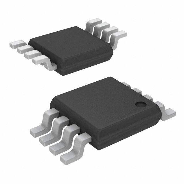
Package 8-TSSOP, 8-MSOP (0.118, 3.00mm Width)
Category Discrete Semiconductor Products / Transistors - FETs, MOSFETs - Single
Description
MOSFET N-CH 20V 5.7A MICRO-8
PDF
/
Inventory: 6413
Minimum: /
The more specific your information, the faster response you will get.
Please complete the following form with the details of your request part and
contact information to get a quote.
Quotation Consultation
Technical Details
Compliance
RoHS Status ROHS3 Compliant
Technical
DS Breakdown Voltage-Min 20V
Pulsed Drain Current-Max (IDM) 30A
Drain-source On Resistance-Max 0.035Ohm
Drain Current-Max (Abs) (ID) 5.7A
Vgs (Max) ±12V
Drive Voltage (Max Rds On,Min Rds On) 2.7V 4.5V
Drain to Source Voltage (Vdss) 20V
Gate Charge (Qg) (Max) @ Vgs 22nC @ 4.5V
Current - Continuous Drain (Id) @ 25°C 5.7A Ta
Input Capacitance (Ciss) (Max) @ Vds 650pF @ 15V
Vgs(th) (Max) @ Id 700mV @ 250μA
Rds On (Max) @ Id, Vgs 35m Ω @ 3.8A, 4.5V
Transistor Application SWITCHING
FET Type N-Channel
Operating Mode ENHANCEMENT MODE
Power Dissipation-Max 1.8W Ta
Configuration SINGLE WITH BUILT-IN DIODE
Number of Elements 1
Qualification Status Not Qualified
JESD-30 Code R-PDSO-G8
Time@Peak Reflow Temperature-Max (s) NOT SPECIFIED
Peak Reflow Temperature (Cel) NOT SPECIFIED
Terminal Form GULL WING
Terminal Position DUAL
Technology MOSFET (Metal Oxide)
Subcategory FET General Purpose Power
Additional Feature HIGH RELIABILITY
ECCN Code EAR99
Number of Terminations 8
Moisture Sensitivity Level (MSL) 1 (Unlimited)
Part Status Discontinued
Series HEXFET?
Published 2005
Packaging Tube
Operating Temperature -55°C~150°C TJ
Physical
Transistor Element Material SILICON
Surface Mount YES
Package / Case 8-TSSOP, 8-MSOP (0.118, 3.00mm Width)
Mounting Type Surface Mount
Alternative Model

Recommended For You

IRF7601PBF+price,IRF7601PBF+datasheet,IRF7601PBF+in stock,buy+IRF7601PBF,finder+IRF7601PBF,IRF7601PBF+tutorials,IRF7601PBF+download