IRF6712STRPBF
RoHS  RoHS compliant
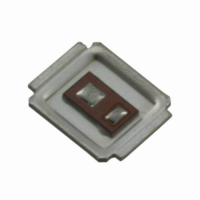
Package DirectFET? Isometric SQ
Category Discrete Semiconductor Products / Transistors - FETs, MOSFETs - Single
Description
MOSFET N-CH 25V 17A DIRECTFET
PDF
/
Buying Options
Total Price: USD $0.51
Unit Price: USD $0.51395
≥1 USD $0.51395
≥10 USD $0.4218
≥100 USD $0.4085
≥500 USD $0.39615
≥1000 USD $0.38285
Inventory: 66517
Minimum: 1
-
+

Technical Details
Compliance
Lead Free Lead Free
RoHS Status ROHS3 Compliant
Radiation Hardening No
Dimensions
Width 3.95mm
Length 4.826mm
Height 506μm
Technical
Drain to Source Breakdown Voltage 25V
Gate to Source Voltage (Vgs) 20V
Continuous Drain Current (ID) 17A
Turn-Off Delay Time 14 ns
Fall Time (Typ) 12 ns
Vgs (Max) ±20V
Drive Voltage (Max Rds On,Min Rds On) 4.5V 10V
Rise Time 40 ns
Gate Charge (Qg) (Max) @ Vgs 18nC @ 4.5V
Current - Continuous Drain (Id) @ 25°C 17A Ta 68A Tc
Input Capacitance (Ciss) (Max) @ Vds 1570pF @ 13V
Vgs(th) (Max) @ Id 2.4V @ 50μA
Rds On (Max) @ Id, Vgs 4.9m Ω @ 17A, 10V
Transistor Application SWITCHING
FET Type N-Channel
Turn On Delay Time 11 ns
Case Connection DRAIN
Power Dissipation 36W
Operating Mode ENHANCEMENT MODE
Power Dissipation-Max 2.2W Ta 36W Tc
Configuration SINGLE WITH BUILT-IN DIODE
Number of Elements 1
JESD-30 Code R-XBCC-N2
Terminal Position BOTTOM
Technology MOSFET (Metal Oxide)
Subcategory FET General Purpose Power
Terminal Finish Tin/Silver/Copper (Sn/Ag/Cu)
Resistance 4.9MOhm
ECCN Code EAR99
Number of Terminations 2
Moisture Sensitivity Level (MSL) 1 (Unlimited)
Part Status Active
JESD-609 Code e1
Series HEXFET?
Published 2009
Packaging Tape & Reel (TR)
Operating Temperature -40°C~150°C TJ
Physical
Transistor Element Material SILICON
Number of Pins 6
Package / Case DirectFET? Isometric SQ
Mounting Type Surface Mount
Mount Surface Mount
Supply Chain
Factory Lead Time 12 Weeks
Alternative Model

Recommended For You

IRF6712STRPBF+price,IRF6712STRPBF+datasheet,IRF6712STRPBF+in stock,buy+IRF6712STRPBF,finder+IRF6712STRPBF,IRF6712STRPBF+tutorials,IRF6712STRPBF+download