IRF3709STRLPBF
RoHS  RoHS compliant
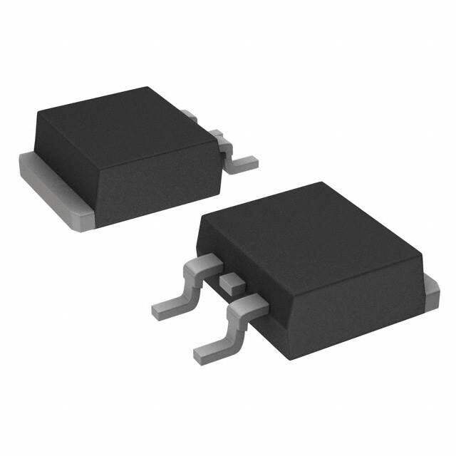
Package TO-263-3, D2Pak (2 Leads + Tab), TO-263AB
Category Discrete Semiconductor Products / Transistors - FETs, MOSFETs - Single
Description
MOSFET N-CH 30V 90A D2PAK
PDF
/
Buying Options
Total Price: USD $1.07
Unit Price: USD $1.07445
≥1 USD $1.07445
≥10 USD $0.8816
≥100 USD $0.85405
≥500 USD $0.8265
≥1000 USD $0.79895
Inventory: 1317
Minimum: 1
-
+

Technical Details
Compliance
RoHS Status ROHS3 Compliant
REACH SVHC No SVHC
Radiation Hardening No
Dimensions
Width 9.65mm
Length 10.668mm
Height 4.826mm
Technical
Nominal Vgs 20 V
Drain to Source Breakdown Voltage 30V
Drain-source On Resistance-Max 0.009Ohm
Drain Current-Max (Abs) (ID) 75A
Gate to Source Voltage (Vgs) 20V
Continuous Drain Current (ID) 90A
Turn-Off Delay Time 21 ns
Fall Time (Typ) 9.2 ns
Vgs (Max) ±20V
Drive Voltage (Max Rds On,Min Rds On) 4.5V 10V
Rise Time 171 ns
Gate Charge (Qg) (Max) @ Vgs 41nC @ 5V
Current - Continuous Drain (Id) @ 25°C 90A Tc
Input Capacitance (Ciss) (Max) @ Vds 2672pF @ 16V
Vgs(th) (Max) @ Id 3V @ 250μA
Rds On (Max) @ Id, Vgs 9m Ω @ 15A, 10V
Transistor Application SWITCHING
FET Type N-Channel
Turn On Delay Time 11 ns
Case Connection DRAIN
Power Dissipation 120W
Operating Mode ENHANCEMENT MODE
Element Configuration Single
Power Dissipation-Max 3.1W Ta 120W Tc
Number of Elements 1
JESD-30 Code R-PSSO-G2
Time@Peak Reflow Temperature-Max (s) 30
Peak Reflow Temperature (Cel) 260
Terminal Form GULL WING
Technology MOSFET (Metal Oxide)
Terminal Finish Matte Tin (Sn) - with Nickel (Ni) barrier
ECCN Code EAR99
Number of Terminations 2
Moisture Sensitivity Level (MSL) 1 (Unlimited)
Part Status Not For New Designs
JESD-609 Code e3
Series HEXFET?
Published 2004
Packaging Tape & Reel (TR)
Operating Temperature -55°C~150°C TJ
Physical
Transistor Element Material SILICON
Number of Pins 3
Package / Case TO-263-3, D2Pak (2 Leads + Tab), TO-263AB
Mounting Type Surface Mount
Mount Surface Mount
Supply Chain
Factory Lead Time 12 Weeks
Alternative Model

Recommended For You

IRF3709STRLPBF+price,IRF3709STRLPBF+datasheet,IRF3709STRLPBF+in stock,buy+IRF3709STRLPBF,finder+IRF3709STRLPBF,IRF3709STRLPBF+tutorials,IRF3709STRLPBF+download