BSP322PH6327XTSA1
RoHS  RoHS compliant
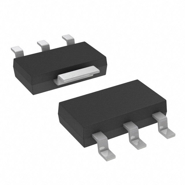
Package TO-261-4, TO-261AA
Category Discrete Semiconductor Products / Transistors - FETs, MOSFETs - Single
Description
Trans MOSFET P-CH 100V 1A Automotive 4-Pin(3+Tab) SOT-223 T/R
PDF
/
Buying Options
Total Price: USD $2.68
Unit Price: USD $2.6847
≥1 USD $2.6847
≥10 USD $2.20305
≥100 USD $2.13465
≥500 USD $2.0653
≥1000 USD $1.9969
≥3000 USD $1.7898
Inventory: 51376
Minimum: 1
-
+

Technical Details
Compliance
Lead Free Lead Free
RoHS Status ROHS3 Compliant
Dimensions
Width 3.5mm
Length 6.5mm
Height 1.6mm
Technical
Drain-source On Resistance-Max 0.8Ohm
Drain Current-Max (Abs) (ID) 1A
Max Dual Supply Voltage -100V
Gate to Source Voltage (Vgs) 20V
Continuous Drain Current (ID) 1A
Turn-Off Delay Time 21.2 ns
Fall Time (Typ) 8.3 ns
Vgs (Max) ±20V
Drive Voltage (Max Rds On,Min Rds On) 4.5V 10V
Drain to Source Voltage (Vdss) 100V
Rise Time 4.3 ns
Gate Charge (Qg) (Max) @ Vgs 16.5nC @ 10V
Current - Continuous Drain (Id) @ 25°C 1A Tc
Input Capacitance (Ciss) (Max) @ Vds 372pF @ 25V
Halogen Free Halogen Free
Vgs(th) (Max) @ Id 1V @ 380μA
Rds On (Max) @ Id, Vgs 800m Ω @ 1A, 10V
FET Type P-Channel
Turn On Delay Time 4.6 ns
Case Connection DRAIN
Power Dissipation 1.8W
Operating Mode ENHANCEMENT MODE
Element Configuration Single
Power Dissipation-Max 1.8W Ta
Number of Elements 1
Pin Count 4
Time@Peak Reflow Temperature-Max (s) NOT SPECIFIED
Peak Reflow Temperature (Cel) NOT SPECIFIED
Terminal Form GULL WING
Terminal Position DUAL
Technology MOSFET (Metal Oxide)
Additional Feature AVALANCHE RATED, LOGIC LEVEL COMPATIBLE
ECCN Code EAR99
Number of Terminations 4
Moisture Sensitivity Level (MSL) 1 (Unlimited)
Part Status Active
Pbfree Code yes
JESD-609 Code e3
Series SIPMOS?
Published 2012
Packaging Cut Tape (CT)
Operating Temperature -55°C~150°C TJ
Physical
Transistor Element Material SILICON
Number of Pins 4
Package / Case TO-261-4, TO-261AA
Mounting Type Surface Mount
Mount Surface Mount
Contact Plating Tin
Supply Chain
Factory Lead Time 10 Weeks
Alternative Model

Recommended For You

BSP322PH6327XTSA1+price,BSP322PH6327XTSA1+datasheet,BSP322PH6327XTSA1+in stock,buy+BSP322PH6327XTSA1,finder+BSP322PH6327XTSA1,BSP322PH6327XTSA1+tutorials,BSP322PH6327XTSA1+download