BSP149 E6327
RoHS
/
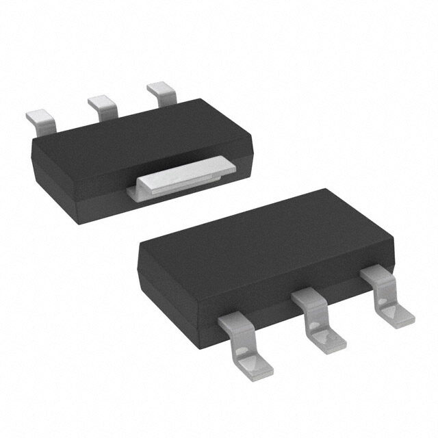
Package TO-261-4, TO-261AA
Category Discrete Semiconductor Products / Transistors - FETs, MOSFETs - Single
Description
MOSFET N-CH 200V 660MA SOT-223
PDF
/
Buying Options
Total Price: USD $1.88
Unit Price: USD $1.88005
≥1 USD $1.88005
≥10 USD $1.5428
≥100 USD $1.49435
≥500 USD $1.44685
≥1000 USD $1.3984
Inventory: 120838
Minimum: 1
-
+

Technical Details
Compliance
RoHS Status Non-RoHS Compliant
Technical
FET Feature Depletion Mode
DS Breakdown Voltage-Min 200V
Pulsed Drain Current-Max (IDM) 1.44A
Drain-source On Resistance-Max 3.5Ohm
Drain Current-Max (Abs) (ID) 0.48A
Vgs (Max) ±20V
Drive Voltage (Max Rds On,Min Rds On) 0V 10V
Drain to Source Voltage (Vdss) 200V
Gate Charge (Qg) (Max) @ Vgs 14nC @ 5V
Current - Continuous Drain (Id) @ 25°C 660mA Ta
Input Capacitance (Ciss) (Max) @ Vds 430pF @ 25V
Vgs(th) (Max) @ Id 1V @ 400μA
Rds On (Max) @ Id, Vgs 1.8 Ω @ 660mA, 10V
FET Type N-Channel
Case Connection DRAIN
Power Dissipation-Max 1.8W Ta
Configuration SINGLE WITH BUILT-IN DIODE
Number of Elements 1
Qualification Status Not Qualified
JESD-30 Code R-PDSO-G4
Pin Count 4
Time@Peak Reflow Temperature-Max (s) NOT SPECIFIED
Peak Reflow Temperature (Cel) 260
Terminal Form GULL WING
Terminal Position DUAL
Technology MOSFET (Metal Oxide)
Subcategory FET General Purpose Power
HTS Code 8541.29.00.95
Terminal Finish Tin/Lead (Sn/Pb)
ECCN Code EAR99
Number of Terminations 4
Moisture Sensitivity Level (MSL) 1 (Unlimited)
Part Status Obsolete
JESD-609 Code e0
Series SIPMOS?
Published 2007
Packaging Tape & Reel (TR)
Operating Temperature -55°C~150°C TJ
Physical
Transistor Element Material SILICON
Surface Mount YES
Package / Case TO-261-4, TO-261AA
Mounting Type Surface Mount
Alternative Model

Recommended For You

BSP149 E6327+price,BSP149 E6327+datasheet,BSP149 E6327+in stock,buy+BSP149 E6327,finder+BSP149 E6327,BSP149 E6327+tutorials,BSP149 E6327+download