AUIRFU3607
RoHS
/
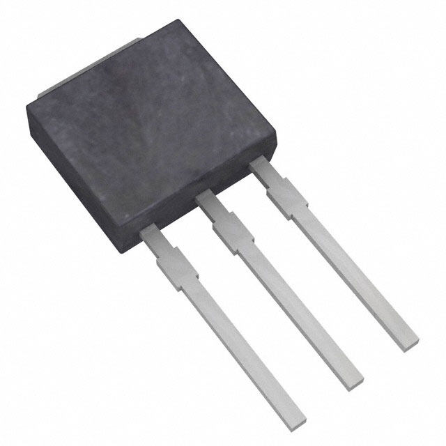
Package TO-251-3 Short Leads, IPak, TO-251AA
Category Discrete Semiconductor Products / Transistors - FETs, MOSFETs - Single
Description
MOSFET N CH 75V 56A I-PAK
PDF
/
Buying Options
Total Price: USD $7.45
Unit Price: USD $7.448
≥1 USD $7.448
≥10 USD $6.11135
≥100 USD $5.9204
≥500 USD $5.72945
≥1000 USD $5.5385
Inventory: 1100
Minimum: 1
-
+

Technical Details
Compliance
Lead Free Lead Free
RoHS Status RoHS Compliant
Radiation Hardening No
Technical
DS Breakdown Voltage-Min 75V
Drain-source On Resistance-Max 0.009Ohm
Drain Current-Max (Abs) (ID) 56A
Gate to Source Voltage (Vgs) 20V
Continuous Drain Current (ID) 80A
Turn-Off Delay Time 43 ns
Fall Time (Typ) 96 ns
Vgs (Max) ±20V
Drive Voltage (Max Rds On,Min Rds On) 10V
Drain to Source Voltage (Vdss) 75V
Rise Time 110 ns
Gate Charge (Qg) (Max) @ Vgs 84nC @ 10V
Current - Continuous Drain (Id) @ 25°C 56A Tc
Input Capacitance (Ciss) (Max) @ Vds 3070pF @ 50V
Vgs(th) (Max) @ Id 4V @ 100μA
Rds On (Max) @ Id, Vgs 9m Ω @ 46A, 10V
Transistor Application SWITCHING
FET Type N-Channel
Turn On Delay Time 16 ns
Case Connection DRAIN
Power Dissipation 140W
Operating Mode ENHANCEMENT MODE
Element Configuration Single
Power Dissipation-Max 140W Tc
Number of Channels 1
Number of Elements 1
Time@Peak Reflow Temperature-Max (s) 30
Peak Reflow Temperature (Cel) 260
Technology MOSFET (Metal Oxide)
Subcategory FET General Purpose Power
Additional Feature HIGH RELIABILITY, ULTRA-LOW RESISTANCE
Terminal Finish Matte Tin (Sn) - with Nickel (Ni) barrier
ECCN Code EAR99
Number of Terminations 3
Moisture Sensitivity Level (MSL) 1 (Unlimited)
Part Status Obsolete
JESD-609 Code e3
Series HEXFET?
Published 2015
Packaging Tube
Operating Temperature -55°C~175°C TJ
Physical
Transistor Element Material SILICON
Number of Pins 3
Package / Case TO-251-3 Short Leads, IPak, TO-251AA
Mounting Type Through Hole
Mount Through Hole
Supply Chain
Factory Lead Time 11 Weeks
Alternative Model

Recommended For You

AUIRFU3607+price,AUIRFU3607+datasheet,AUIRFU3607+in stock,buy+AUIRFU3607,finder+AUIRFU3607,AUIRFU3607+tutorials,AUIRFU3607+download