DMN3024LK3-13
RoHS  RoHS compliant
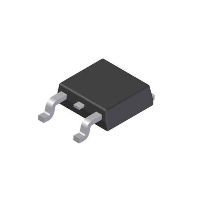
Package TO-252-3, DPak (2 Leads + Tab), SC-63
Category Discrete Semiconductor Products / Transistors - FETs, MOSFETs - Single
Description
MOSFET N-CH 30V 9.78A DPAK
PDF
/
Buying Options
Total Price: USD $0.49
Unit Price: USD $0.4928
≥1 USD $0.4928
≥10 USD $0.41888
≥100 USD $0.291192
≥500 USD $0.227339
≥1000 USD $0.184782
Inventory: 1094
Minimum: 1
-
+

Technical Details
Compliance
RoHS Status ROHS3 Compliant
REACH SVHC No SVHC
Radiation Hardening No
Dimensions
Width 6.22mm
Length 6.73mm
Height 2.39mm
Technical
Pulsed Drain Current-Max (IDM) 46.5A
Drain-source On Resistance-Max 0.024Ohm
Drain Current-Max (Abs) (ID) 9.78A
Gate to Source Voltage (Vgs) 20V
JEDEC-95 Code TO-252AA
Continuous Drain Current (ID) 14.4A
Turn-Off Delay Time 16 ns
Fall Time (Typ) 8 ns
Vgs (Max) ±20V
Drive Voltage (Max Rds On,Min Rds On) 4.5V 10V
Drain to Source Voltage (Vdss) 30V
Rise Time 3.3 ns
Gate Charge (Qg) (Max) @ Vgs 12.9nC @ 10V
Current - Continuous Drain (Id) @ 25°C 9.78A Ta
Input Capacitance (Ciss) (Max) @ Vds 608pF @ 15V
Vgs(th) (Max) @ Id 3V @ 250μA
Rds On (Max) @ Id, Vgs 24m Ω @ 7A, 10V
Transistor Application SWITCHING
FET Type N-Channel
Turn On Delay Time 2.9 ns
Case Connection DRAIN
Power Dissipation 8.9W
Operating Mode ENHANCEMENT MODE
Element Configuration Single
Power Dissipation-Max 2.17W Ta
Number of Channels 1
Number of Elements 1
JESD-30 Code R-PSSO-G2
Pin Count 3
Time@Peak Reflow Temperature-Max (s) 40
Peak Reflow Temperature (Cel) 260
Terminal Form GULL WING
Technology MOSFET (Metal Oxide)
Subcategory FET General Purpose Power
Terminal Finish Matte Tin (Sn)
ECCN Code EAR99
Number of Terminations 2
Moisture Sensitivity Level (MSL) 1 (Unlimited)
Part Status Active
Pbfree Code no
JESD-609 Code e3
Packaging Cut Tape (CT)
Operating Temperature -55°C~150°C TJ
Physical
Transistor Element Material SILICON
Weight 3.949996g
Number of Pins 3
Package / Case TO-252-3, DPak (2 Leads + Tab), SC-63
Mounting Type Surface Mount
Mount Surface Mount
Supply Chain
Factory Lead Time 17 Weeks
Alternative Model

Recommended For You

DMN3024LK3-13+price,DMN3024LK3-13+datasheet,DMN3024LK3-13+in stock,buy+DMN3024LK3-13,finder+DMN3024LK3-13,DMN3024LK3-13+tutorials,DMN3024LK3-13+download