STL50DN6F7
RoHS  RoHS compliant
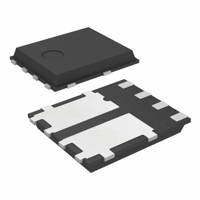
Package 8-PowerVDFN
Category Discrete Semiconductor Products / Transistors - FETs, MOSFETs - Arrays
Description
MOSFET N-CH 60V 57A POWERFLAT
PDF
/
Buying Options
Total Price: USD $1.42
Unit Price: USD $1.4168
≥1 USD $1.4168
≥10 USD $1.16248
≥100 USD $0.904112
≥500 USD $0.766357
≥1000 USD $0.624272
Inventory: 1703
Minimum: 1
-
+

Technical Details
Compliance
Lead Free Lead Free
RoHS Status ROHS3 Compliant
Technical
FET Feature Standard
FET Technology METAL-OXIDE SEMICONDUCTOR
DS Breakdown Voltage-Min 60V
Drain-source On Resistance-Max 0.011Ohm
Continuous Drain Current (ID) 57A
Drain to Source Voltage (Vdss) 60V
Gate Charge (Qg) (Max) @ Vgs 17nC @ 10V
Current - Continuous Drain (Id) @ 25°C 57A Tc
Input Capacitance (Ciss) (Max) @ Vds 1035pF @ 30V
Vgs(th) (Max) @ Id 4V @ 250μA
Rds On (Max) @ Id, Vgs 11m Ω @ 7.5A, 10V
Transistor Application SWITCHING
FET Type 2 N-Channel (Dual)
Case Connection DRAIN
Operating Mode ENHANCEMENT MODE
Configuration SEPARATE, 2 ELEMENTS WITH BUILT-IN DIODE
Number of Elements 2
JESD-30 Code R-PDSO-F6
Base Part Number STL50
Time@Peak Reflow Temperature-Max (s) NOT SPECIFIED
Reach Compliance Code not_compliant
Peak Reflow Temperature (Cel) 260
Terminal Form FLAT
Max Power Dissipation 62.5W
Terminal Finish Matte Tin (Sn)
ECCN Code EAR99
Number of Terminations 6
Moisture Sensitivity Level (MSL) 1 (Unlimited)
Part Status Active
JESD-609 Code e3
Series STripFET?
Packaging Tape & Reel (TR)
Operating Temperature -55°C~175°C TJ
Physical
Transistor Element Material SILICON
Number of Pins 8
Package / Case 8-PowerVDFN
Mounting Type Surface Mount
Mount Surface Mount
Supply Chain
Lifecycle Status ACTIVE (Last Updated: 8 months ago)
Alternative Model

Recommended For You

STL50DN6F7+price,STL50DN6F7+datasheet,STL50DN6F7+in stock,buy+STL50DN6F7,finder+STL50DN6F7,STL50DN6F7+tutorials,STL50DN6F7+download