STC6NF30V
RoHS  RoHS compliant
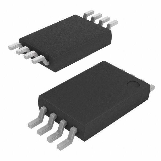
Package 8-TSSOP (0.173, 4.40mm Width)
Category Discrete Semiconductor Products / Transistors - FETs, MOSFETs - Arrays
Description
MOSFET N-Ch 30 Volt 6 Amp
PDF
/
Inventory: 5908
Minimum: /
The more specific your information, the faster response you will get.
Please complete the following form with the details of your request part and
contact information to get a quote.
Quotation Consultation
Technical Details
Compliance
RoHS Status ROHS3 Compliant
Radiation Hardening No
Technical
FET Feature Logic Level Gate
FET Technology METAL-OXIDE SEMICONDUCTOR
Drain to Source Breakdown Voltage 30V
Drain-source On Resistance-Max 0.03Ohm
Drain Current-Max (Abs) (ID) 6A
Gate to Source Voltage (Vgs) 12V
Continuous Drain Current (ID) 6A
Turn-Off Delay Time 32 ns
Fall Time (Typ) 25 ns
Rise Time 25ns
Gate Charge (Qg) (Max) @ Vgs 9nC @ 2.5V
Input Capacitance (Ciss) (Max) @ Vds 800pF @ 25V
Vgs(th) (Max) @ Id 600mV @ 250μA
Rds On (Max) @ Id, Vgs 25m Ω @ 3A, 4.5V
Transistor Application SWITCHING
FET Type 2 N-Channel (Dual)
Turn On Delay Time 20 ns
Power Dissipation 1.5W
Operating Mode ENHANCEMENT MODE
Number of Elements 2
Pin Count 8
Base Part Number STC6NF
Time@Peak Reflow Temperature-Max (s) 10
Current Rating 6A
Peak Reflow Temperature (Cel) 260
Terminal Form GULL WING
Max Power Dissipation 1.5W
Voltage - Rated DC 30V
Subcategory FET General Purpose Power
Additional Feature LOW THRESHOLD
Terminal Finish Nickel/Palladium/Gold (Ni/Pd/Au)
ECCN Code EAR99
Number of Terminations 8
Moisture Sensitivity Level (MSL) 1 (Unlimited)
Part Status Obsolete
JESD-609 Code e4
Series STripFET? II
Packaging Tape & Reel (TR)
Operating Temperature -55°C~150°C TJ
Physical
Transistor Element Material SILICON
Number of Pins 8
Package / Case 8-TSSOP (0.173, 4.40mm Width)
Mounting Type Surface Mount
Mount Surface Mount
Alternative Model

Recommended For You

STC6NF30V+price,STC6NF30V+datasheet,STC6NF30V+in stock,buy+STC6NF30V,finder+STC6NF30V,STC6NF30V+tutorials,STC6NF30V+download