TT8J2TR
RoHS  RoHS compliant
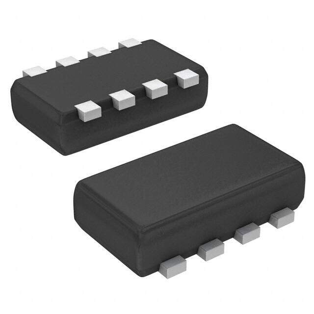
Package 8-SMD, Flat Lead
Category Discrete Semiconductor Products / Transistors - FETs, MOSFETs - Arrays
Description
MOSFET 2P-CH 30V 2.5A TSST8
PDF
/
Buying Options
Total Price: USD $0.63
Unit Price: USD $0.63124
≥1 USD $0.63124
≥10 USD $0.59551
≥100 USD $0.5618
≥500 USD $0.53
≥1000 USD $0.5
Inventory: 1600
Minimum: 1
-
+

Technical Details
Compliance
Lead Free Lead Free
RoHS Status ROHS3 Compliant
Radiation Hardening No
Technical
FET Feature Logic Level Gate
FET Technology METAL-OXIDE SEMICONDUCTOR
Pulsed Drain Current-Max (IDM) 10A
Drain to Source Breakdown Voltage -30V
Gate to Source Voltage (Vgs) 20V
Continuous Drain Current (ID) 2.5A
Turn-Off Delay Time 35 ns
Fall Time (Typ) 14 ns
Drain to Source Voltage (Vdss) 30V
Rise Time 20ns
Gate Charge (Qg) (Max) @ Vgs 4.8nC @ 5V
Input Capacitance (Ciss) (Max) @ Vds 460pF @ 10V
Vgs(th) (Max) @ Id 2.5V @ 1mA
Rds On (Max) @ Id, Vgs 84m Ω @ 2.5A, 10V
Transistor Application SWITCHING
FET Type 2 P-Channel (Dual)
Turn On Delay Time 7 ns
Power Dissipation 1.25W
Operating Mode ENHANCEMENT MODE
Configuration SEPARATE, 2 ELEMENTS WITH BUILT-IN DIODE
Number of Elements 2
Pin Count 8
Base Part Number *J2
Time@Peak Reflow Temperature-Max (s) 10
Peak Reflow Temperature (Cel) 260
Max Power Dissipation 1.25W
Terminal Finish TIN COPPER
ECCN Code EAR99
Number of Terminations 8
Moisture Sensitivity Level (MSL) 1 (Unlimited)
Part Status Not For New Designs
Pbfree Code yes
JESD-609 Code e2
Published 2009
Packaging Tape & Reel (TR)
Operating Temperature 150°C TJ
Physical
Transistor Element Material SILICON
Number of Pins 8
Package / Case 8-SMD, Flat Lead
Mounting Type Surface Mount
Mount Surface Mount
Supply Chain
Factory Lead Time 10 Weeks
Alternative Model

Recommended For You

TT8J2TR+price,TT8J2TR+datasheet,TT8J2TR+in stock,buy+TT8J2TR,finder+TT8J2TR,TT8J2TR+tutorials,TT8J2TR+download