QS6M4TR
RoHS  RoHS compliant
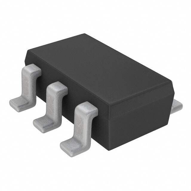
Package SOT-23-6 Thin, TSOT-23-6
Category Discrete Semiconductor Products / Transistors - FETs, MOSFETs - Arrays
Description
MOSFET N/P-CH 30V/20V 1.5A TSMT6
PDF
/
Buying Options
Total Price: USD $0.51
Unit Price: USD $0.5104
≥1 USD $0.5104
≥10 USD $0.43912
≥100 USD $0.303952
≥500 USD $0.253986
≥1000 USD $0.216154
Inventory: 1250
Minimum: 1
-
+

Technical Details
Compliance
Lead Free Lead Free
RoHS Status ROHS3 Compliant
Radiation Hardening No
Technical
FET Feature Logic Level Gate
FET Technology METAL-OXIDE SEMICONDUCTOR
Drain to Source Breakdown Voltage -20V
Drain-source On Resistance-Max 0.245Ohm
Gate to Source Voltage (Vgs) 12V
Threshold Voltage 1.5V
Continuous Drain Current (ID) 1.5A
Turn-Off Delay Time 45 ns
Fall Time (Typ) 12 ns
Polarity/Channel Type N-CHANNEL AND P-CHANNEL
Drain to Source Voltage (Vdss) 30V 20V
Rise Time 12 ns
Gate Charge (Qg) (Max) @ Vgs 1.6nC @ 4.5V
Input Capacitance (Ciss) (Max) @ Vds 80pF @ 10V
Vgs(th) (Max) @ Id 1.5V @ 1mA
Rds On (Max) @ Id, Vgs 230m Ω @ 1.5A, 4.5V
Transistor Application SWITCHING
FET Type N and P-Channel
Power Dissipation 1.25W
Operating Mode ENHANCEMENT MODE
Element Configuration Dual
Number of Elements 2
Pin Count 6
Base Part Number *M4
Time@Peak Reflow Temperature-Max (s) 10
Current Rating 1.5A
Peak Reflow Temperature (Cel) 260
Terminal Form GULL WING
Max Power Dissipation 1.25W
Subcategory Other Transistors
HTS Code 8541.29.00.95
ECCN Code EAR99
Number of Terminations 6
Moisture Sensitivity Level (MSL) 1 (Unlimited)
Part Status Active
Pbfree Code yes
JESD-609 Code e1
Published 2006
Packaging Tape & Reel (TR)
Operating Temperature 150°C TJ
Physical
Transistor Element Material SILICON
Number of Pins 6
Package / Case SOT-23-6 Thin, TSOT-23-6
Mounting Type Surface Mount
Mount Surface Mount
Supply Chain
Factory Lead Time 20 Weeks
Alternative Model

Recommended For You

QS6M4TR+price,QS6M4TR+datasheet,QS6M4TR+in stock,buy+QS6M4TR,finder+QS6M4TR,QS6M4TR+tutorials,QS6M4TR+download