FDJ1027P
RoHS  RoHS compliant
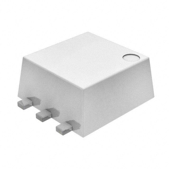
Package SC75-6 FLMP
Category Discrete Semiconductor Products / Transistors - FETs, MOSFETs - Arrays
Description
P-CHANNEL POWER MOSFET
PDF
/
Buying Options
Total Price: USD $0.28
Unit Price: USD $0.2816
≥1 USD $0.2816
Inventory: 283352
Minimum: 1
-
+

Technical Details
Compliance
RoHS Status ROHS3 Compliant
Technical
FET Feature Logic Level Gate
FET Technology METAL-OXIDE SEMICONDUCTOR
DS Breakdown Voltage-Min 20V
Pulsed Drain Current-Max (IDM) 12A
Drain-source On Resistance-Max 0.16Ohm
Drain Current-Max (Abs) (ID) 2.8A
Drain to Source Voltage (Vdss) 20V
Gate Charge (Qg) (Max) @ Vgs 4nC @ 4.5V
Current - Continuous Drain (Id) @ 25°C 2.8A
Input Capacitance (Ciss) (Max) @ Vds 290pF @ 10V
Vgs(th) (Max) @ Id 1.5V @ 250μA
Rds On (Max) @ Id, Vgs 160m Ω @ 2.8A, 4.5V
Transistor Application SWITCHING
FET Type 2 P-Channel (Dual)
Power - Max 900mW
Case Connection DRAIN
Operating Mode ENHANCEMENT MODE
Configuration SEPARATE, 2 ELEMENTS WITH BUILT-IN DIODE
Number of Elements 2
Qualification Status COMMERCIAL
JESD-30 Code R-PDSO-F6
Pin Count 6
Time@Peak Reflow Temperature-Max (s) NOT SPECIFIED
Reach Compliance Code unknown
Peak Reflow Temperature (Cel) NOT SPECIFIED
Terminal Form FLAT
Terminal Finish NICKEL PALLADIUM GOLD
Number of Terminations 6
Moisture Sensitivity Level (MSL) 1 (Unlimited)
Part Status Obsolete
Pbfree Code yes
JESD-609 Code e4
Series PowerTrench?
Packaging Tape & Reel (TR)
Operating Temperature -55°C~150°C TJ
Physical
Transistor Element Material SILICON
Surface Mount YES
Package / Case SC75-6 FLMP
Mounting Type Surface Mount
Alternative Model

Recommended For You

FDJ1027P+price,FDJ1027P+datasheet,FDJ1027P+in stock,buy+FDJ1027P,finder+FDJ1027P,FDJ1027P+tutorials,FDJ1027P+download