FDMD84100
RoHS  RoHS compliant
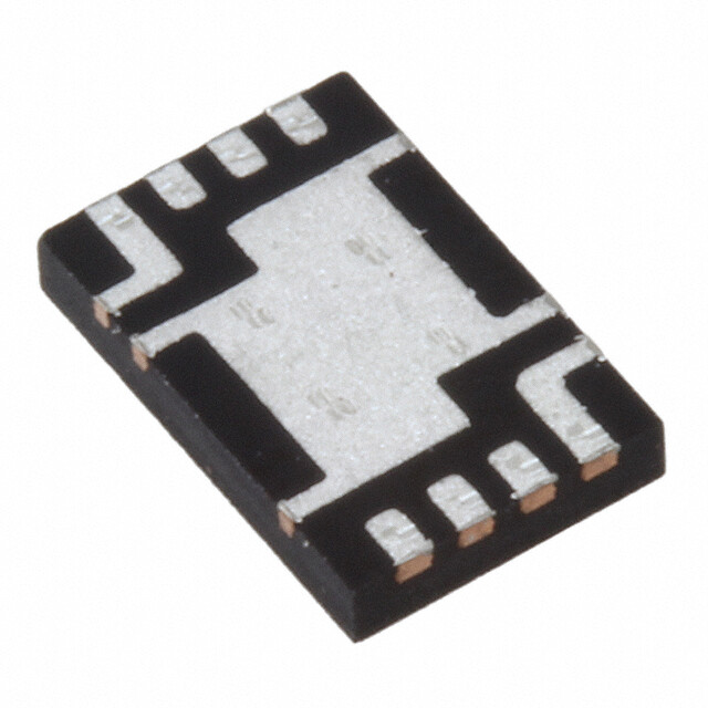
Package 8-PowerWDFN
Category Discrete Semiconductor Products / Transistors - FETs, MOSFETs - Arrays
Description
MOSFET 2N-CH 100V 7A 8-PQFN
PDF
/
Buying Options
Total Price: USD $2.72
Unit Price: USD $2.717032
≥1 USD $2.717032
≥10 USD $2.56324
≥100 USD $2.418145
≥500 USD $2.281273
≥1000 USD $2.152145
Inventory: 1286
Minimum: 1
-
+

Technical Details
Compliance
RoHS Status ROHS3 Compliant
Dimensions
Width 3.4mm
Length 5.1mm
Height 750μm
Technical
FET Feature Standard
FET Technology METAL-OXIDE SEMICONDUCTOR
Drain to Source Breakdown Voltage 100V
Drain Current-Max (Abs) (ID) 7A
Gate to Source Voltage (Vgs) 20V
Continuous Drain Current (ID) 21A
Turn-Off Delay Time 14 ns
Fall Time (Typ) 2.8 ns
Rise Time 2.6 ns
Gate Charge (Qg) (Max) @ Vgs 16nC @ 10V
Current - Continuous Drain (Id) @ 25°C 7A
Input Capacitance (Ciss) (Max) @ Vds 980pF @ 50V
Vgs(th) (Max) @ Id 4V @ 250μA
Rds On (Max) @ Id, Vgs 20m Ω @ 7A, 10V
Transistor Application SWITCHING
FET Type 2 N-Channel (Dual) Common Source
Power - Max 2.1W
Turn On Delay Time 8.4 ns
Operating Mode ENHANCEMENT MODE
Element Configuration Dual
Number of Channels 2
Number of Elements 2
Time@Peak Reflow Temperature-Max (s) NOT SPECIFIED
Reach Compliance Code not_compliant
Peak Reflow Temperature (Cel) NOT SPECIFIED
Terminal Form NO LEAD
Max Power Dissipation 23W
Subcategory FET General Purpose Power
Terminal Finish Tin (Sn)
ECCN Code EAR99
Number of Terminations 8
Moisture Sensitivity Level (MSL) 1 (Unlimited)
Part Status Active
Pbfree Code yes
JESD-609 Code e3
Series PowerTrench?
Published 2017
Packaging Tape & Reel (TR)
Operating Temperature -55°C~150°C TJ
Physical
Transistor Element Material SILICON
Weight 153.4014mg
Number of Pins 8
Package / Case 8-PowerWDFN
Mounting Type Surface Mount
Mount Surface Mount
Supply Chain
Lifecycle Status ACTIVE (Last Updated: 1 day ago)
Factory Lead Time 12 Weeks
Alternative Model

Recommended For You

FDMD84100+price,FDMD84100+datasheet,FDMD84100+in stock,buy+FDMD84100,finder+FDMD84100,FDMD84100+tutorials,FDMD84100+download