STL7N80K5
RoHS  RoHS compliant
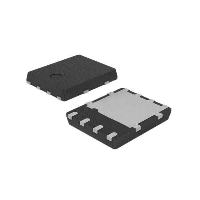
Package 8-PowerVDFN
Category Discrete Semiconductor Products / Transistors - FETs, MOSFETs - Single
Description
MOSFET N-CH 800V 8POWERFLAT
PDF
/
Buying Options
Total Price: USD $2.01
Unit Price: USD $2.0064
≥1 USD $2.0064
≥10 USD $1.66848
≥100 USD $1.327656
≥500 USD $1.123408
≥1000 USD $0.953198
Inventory: 1484
Minimum: 1
-
+

Technical Details
Compliance
Lead Free Lead Free
RoHS Status ROHS3 Compliant
Dimensions
Width 5.4mm
Length 6.35mm
Height 950μm
Technical
Gate to Source Voltage (Vgs) 30V
Continuous Drain Current (ID) 3.6A
Turn-Off Delay Time 23.7 ns
Fall Time (Typ) 20.2 ns
Vgs (Max) ±30V
Drive Voltage (Max Rds On,Min Rds On) 10V
Drain to Source Voltage (Vdss) 800V
Rise Time 8.3 ns
Gate Charge (Qg) (Max) @ Vgs 13.4nC @ 10V
Current - Continuous Drain (Id) @ 25°C 3.6A Tc
Input Capacitance (Ciss) (Max) @ Vds 360pF @ 100V
Vgs(th) (Max) @ Id 5V @ 100μA
Rds On (Max) @ Id, Vgs 1.2 Ω @ 3A, 10V
Transistor Application SWITCHING
FET Type N-Channel
Turn On Delay Time 11.3 ns
Case Connection DRAIN
Power Dissipation 42W
Operating Mode ENHANCEMENT MODE
Element Configuration Single
Power Dissipation-Max 42W Tc
Number of Channels 1
Number of Elements 1
JESD-30 Code R-PDSO-F5
Base Part Number STL7
Time@Peak Reflow Temperature-Max (s) NOT SPECIFIED
Peak Reflow Temperature (Cel) NOT SPECIFIED
Terminal Form FLAT
Terminal Position DUAL
Technology MOSFET (Metal Oxide)
Subcategory FET General Purpose Power
ECCN Code EAR99
Number of Terminations 5
Moisture Sensitivity Level (MSL) 1 (Unlimited)
Part Status Active
Series SuperMESH5?
Packaging Tape & Reel (TR)
Operating Temperature -55°C~150°C TJ
Physical
Transistor Element Material SILICON
Number of Pins 8
Package / Case 8-PowerVDFN
Mounting Type Surface Mount
Mount Surface Mount
Supply Chain
Lifecycle Status ACTIVE (Last Updated: 8 months ago)
Factory Lead Time 17 Weeks
Alternative Model

Recommended For You

STL7N80K5+price,STL7N80K5+datasheet,STL7N80K5+in stock,buy+STL7N80K5,finder+STL7N80K5,STL7N80K5+tutorials,STL7N80K5+download