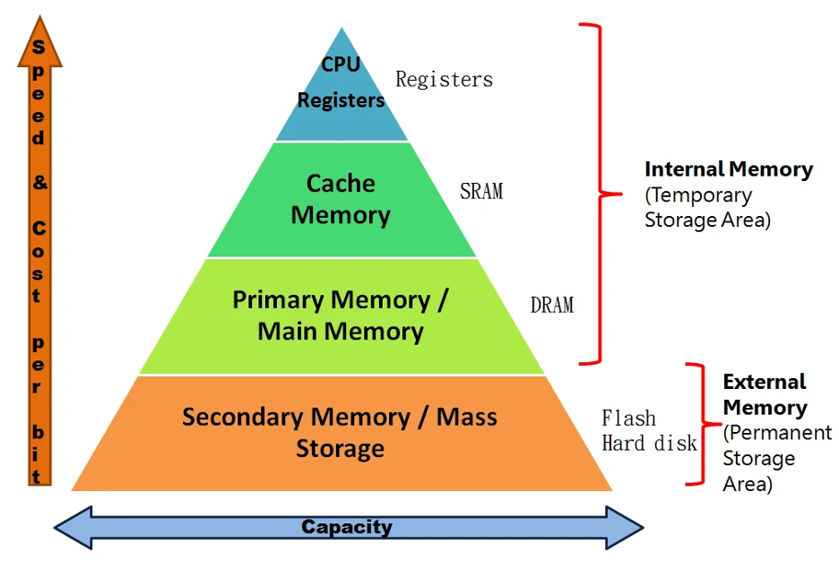
Most modern systems rely on a memory hierarchy because no single technology can deliver high speed, large capacity, and low cost at the same time.
Small, fast SRAM sits close to the CPU as cache memory, while larger DRAM serves as main memory. This speed, capacity, and cost trade-off is why the SRAM vs DRAM comparison still matters in real hardware design.
Choosing between static RAM vs dynamic RAM is not just a component cost decision. A DRAM-based design requires activate, read, write, precharge, and refresh operations, along with memory controller setup and high-speed PCB routing.
An SRAM-based design offers simpler timing and more deterministic access, but lower density and higher cost per bit.
Many guides reduce the difference between SRAM and DRAM to “SRAM is faster, DRAM is cheaper.” The real reason lies in DRAM row and bank sequencing, which makes latency vs bandwidth very different concepts.
Power is also often oversimplified. Large SRAM arrays suffer from leakage, while DRAM consumes refresh power that increases with temperature.
This article explains SRAM vs DRAM architecture, read behavior, latency, power consumption, system cost, and practical selection guidance for embedded and high-performance systems.
TL;DR
SRAM stores bits in latches, which gives it low and predictable latency. That is why it is used for cache memory and other “close-to-CPU” structures.
DRAM stores bits as charge in capacitors. This enables high density and lower cost per bit. However, refresh and command-based access introduce background overhead and higher first-byte latency. That is why modern systems combine DRAM main memory with SRAM caches.
What is SRAM
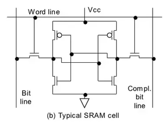
Static random-access memory (SRAM) is a type of volatile memory that stores each bit in a bistable latch. It does not require refresh as long as power is applied.

Once power is removed, the stored data is lost. The most common implementation is the 6-transistor (6T) SRAM cell.
Two cross-coupled inverters hold the logic state, and two access transistors connect the cell to differential bitlines when the wordline is asserted.
During a read, the bitlines are precharged and the wordline is enabled. The stored value creates a small voltage difference, which sense circuitry amplifies into a valid logic level.
During a write, complementary values are driven onto the bitlines and the latch is forced into the new state.
SRAM is deployed where low latency and high access rate matter:
- CPU cache memory and register files
- On-chip scratchpads
- Microcontroller internal SRAM for stack and variables
- Embedded memory blocks in FPGAs and SoCs
These applications rely on SRAM because it delivers fast, predictable access close to the compute core.
In programmable logic and FPGA platforms, on-chip SRAM blocks are used for embedded memory arrays and buffering.
What is DRAM
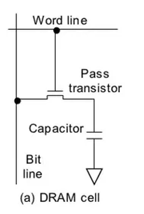
Dynamic random-access memory (DRAM) is a type of volatile memory that stores each bit as charge in a 1T1C cell — one transistor and one capacitor.
Because charge naturally leaks, DRAM must be refreshed periodically to retain data. If refresh stops or power is removed, the data is lost.
DRAM is optimized for high density and low cost per bit, which is why it is widely used as main memory.
In the 1T1C design, writing a bit charges or discharges a tiny capacitor. The access transistor connects the cell to the bitline when the wordline is enabled.
Over time, leakage causes the stored charge to decay.
Retention time varies due to process differences and temperature. Some cells leak faster than others, so refresh timing is designed to handle worst-case conditions.
SRAM vs DRAM Core Architecture Difference
At the most basic level, SRAM stores a bit in a stable latch, while DRAM stores a bit as charge in a capacitor. SRAM holds its state as long as power is present.
DRAM charge leaks over time and must be refreshed.
That single architectural difference drives three system-level outcomes.
1. Density and cost per bit
DRAM’s 1T1C structure enables high bit density and lower cost per bit. SRAM requires multiple transistors per bit, which increases silicon area and limits scalability for large capacities.
2. Interface semantics
SRAM can behave like a straightforward “address to data” memory, especially in simpler implementations. DRAM operates through a command-based protocol built around banks, rows, and columns.
3. Background activity
DRAM must perform refresh and manage row activation and precharge cycles, even when the CPU is idle. SRAM does not require refresh, but large SRAM arrays can suffer from leakage in advanced process nodes.
What Actually Happens During a Read
Understanding the internal read path explains why SRAM vs DRAM speed differs in practice.
SRAM Read Cycle
A typical SRAM read is direct and low latency:
- Bitlines are precharged.
- The wordline connects the cell to the bitlines.
- The stored value creates a small voltage difference.
- A sense amplifier resolves the value.
There are delays from decoders and bitline capacitance, but there is no row activation phase and no refresh-driven blocking.
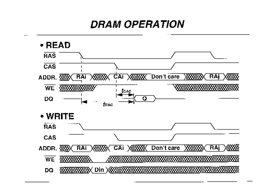
DRAM Read Cycle
A DRAM bank is organized as rows and columns, and its sense amplifiers act as a row buffer. A read from a closed row generally involves:
- ACTIVATE: open the row and load it into the row buffer.
- READ: select the desired column data.
- PRECHARGE: close the row before opening another.
If multiple reads target the same open row, they are faster than switching to a different row.
First-Byte Latency vs Sustained Bandwidth
DRAM performance depends heavily on row state:
- A row hit mostly pays the column delay.
- A row miss requires precharge plus activate plus column delay.
Once a row is open, DRAM can stream burst transfers efficiently. This is why DRAM often delivers high sustained bandwidth per system cost, even though SRAM typically provides lower raw access latency.
SRAM vs DRAM speed
When people compare SRAM vs DRAM speed, they often mean one thing: “SRAM is faster.” That is usually true for latency, but it is not the full story.
In real systems, SRAM tends to win on time-to-data, while DRAM often wins on sustained throughput because it is built to move large blocks efficiently.
Latency
Cache memory exists to reduce average access time by serving most requests from small, fast SRAM structures.
That’s why computer architecture models place SRAM caches above DRAM main memory in the memory hierarchy.
A common way to express this is mean access time:
- t_avg = t_hit + miss_rate × miss_penalty
Here, t_hit is the SRAM cache access time, and the miss penalty is dominated by going to DRAM and beyond. This is also why cache hits feel “instant” compared to main memory.
Even discrete SRAM devices reflect this design goal. Many asynchronous SRAM parts are specified with access times in the single-digit to low double-digit nanosecond range for faster speed grades.
The key idea is simple: SRAM is built to return a word quickly and predictably.
Bandwidth
DRAM is not optimized for the shortest possible access to a random word. It is optimized to deliver high bandwidth once it gets going. Modern DDR memory achieves this using:
- Parallelism across channels, ranks, banks, and bank groups
- Burst transfers that move multiple beats per command
- Row-buffer locality, where repeated accesses to an open row are much cheaper than switching rows
Row behavior matters because opening a row effectively loads a “page” into the row buffer. If your access pattern has locality, DRAM can stream data at very high rates.
Memory controllers also reorder requests to reduce expensive row switches, which helps DRAM deliver strong real-world throughput.
This is why DRAM can look “slow” on first-byte latency but still dominate on sustained bandwidth in systems that process large buffers, frames, and datasets.
Why CPUs Use SRAM Caches Instead of DRAM Directly
This comes down to the classic “memory wall” problem. CPU cores have improved much faster than DRAM latency, so a design that depends on DRAM for every load would stall constantly. SRAM cache memory bridges that gap by keeping hot data close to the CPU.
At the same time, caches cannot scale to DRAM-like capacities. SRAM is limited by silicon area and power, especially leakage in large arrays. So the modern design pattern remains stable:
- SRAM for low-latency caches and near-compute working data
- DRAM for large, cost-effective main memory with high throughput
SRAM vs DRAM Power consumption
Power analysis in SRAM vs DRAM only makes sense when you separate active energy from standby energy. Temperature must also be treated as a real factor, not a footnote.
Both memory types consume power differently, and the result depends on size and workload.
Active Power
DRAM access includes multiple phases. A row must be activated, data is transferred in bursts, and the row may need to be precharged before another is opened. Each of these steps consumes energy. This is why memory controllers try to reduce unnecessary row switches. Fewer activate and precharge cycles mean less wasted energy.
SRAM has no activate or refresh phase. However, reads and writes still require charging and discharging bitlines. Large bitline capacitance makes switching expensive if not carefully designed. At high access rates, SRAM dynamic power becomes significant.
Standby Power
DRAM consumes background power because it must refresh periodically. Refresh takes time and energy, and it reduces memory availability during that interval. This cost exists even when the processor is idle.
SRAM does not refresh, but leakage current is a major concern in large arrays. In advanced process nodes, leakage can represent a meaningful share of total chip power.
Temperature
As temperature rises, leakage increases. For DRAM, this reduces retention time and requires more frequent refresh. More frequent refresh increases energy use and can reduce effective availability. This makes thermal conditions directly relevant to memory power planning.
Practical View
There is no universal low-power winner.
- Small, frequently accessed memory often favors SRAM because it avoids refresh.
- Large memory capacity typically requires DRAM, which is energy-efficient per bit but carries refresh overhead.
- Very large SRAM arrays can suffer from leakage-dominated idle power.
In practice, power efficiency depends on memory size, duty cycle, and operating temperature.
DRAM vs SRAM Cost
Cost comparisons between DRAM vs SRAM are often reduced to “DRAM is cheaper.” That is only partially true. DRAM is usually cheaper per bit, but the full system cost includes controller design, PCB complexity, validation time, and integration risk. A proper comparison must separate device cost from subsystem cost.
Cost per Bit and Density
The core difference starts at the memory cell.
DRAM uses a compact capacitor-based cell, which enables high bit density. More bits fit into the same silicon area, which lowers cost per bit as capacity scales. This is why DRAM dominates when memory requirements reach megabytes or gigabytes.
SRAM uses multiple transistors per bit. The larger cell size increases die area, and since wafer cost scales with area, SRAM has a higher cost per bit at comparable process technology.
In practice:
- SRAM is viable for small memory blocks
- DRAM becomes far more economical for large capacity memory
Controller and Integration Cost
The chip price is only one part of the equation.
A typical SRAM interface can be relatively simple. Address, data, and control signals are often sufficient, and timing is straightforward.
A DRAM subsystem requires:
- A memory controller that manages channels, ranks, banks, rows, and columns
- Refresh scheduling
- Strict timing parameter handling
- Request reordering for efficiency
Modern DRAM also requires PHY training and calibration, such as read/write alignment and delay tuning. This adds engineering time during bring-up and validation.
So while DRAM may reduce cost per bit, it increases integration complexity.
PCB and Signal Integrity Cost
External DRAM operates at high data rates. This introduces strict PCB requirements:
- Controlled impedance routing
- Length matching for data and strobe lines
- Defined routing topologies
- Tight skew margins
Meeting these constraints may require extra PCB layers, simulation work, and extended validation. In many embedded designs, DDR layout becomes one of the most challenging parts of board development.
Chip Cost vs System Cost
When comparing SRAM vs DRAM cost, separate:
- Chip cost — DRAM is usually cheaper per bit
- System cost — DRAM often demands more engineering time, PCB effort, and validation
SRAM has a higher per-bit price but can simplify the overall system. DRAM reduces memory cost at scale but increases subsystem complexity. The correct choice depends on memory size, software requirements, performance goals, and available engineering resources.
DRAM Family Map
When discussing SRAM vs DRAM, it is important to understand that DRAM is not a single product. It is a group of standards designed for different markets. The differences are driven by bandwidth, power targets, packaging constraints, and system architecture.
DDR SDRAM
DDR SDRAM is the mainstream choice for desktops, servers, and many embedded processors. It is optimized for:
- High capacity
- Strong ecosystem support
- Balanced latency and bandwidth
Recent generations such as DDR5 increase bandwidth through higher data rates and architectural changes. These include independent subchannels per DIMM and burst behavior that aligns efficiently with typical cache-line transfers.
DDR is usually selected when capacity and compatibility matter more than extreme power savings.
LPDDR
LPDDR (Low-Power DDR) targets mobile and embedded platforms where power efficiency is critical. It includes power-saving modes and flexible refresh behavior to reduce energy use.
Recent versions such as LPDDR5 and LPDDR5X push higher data rates while maintaining energy efficiency. The newer LPDDR6 standard continues this trend, targeting performance improvements for mobile and AI-oriented devices.
LPDDR integration can be more complex than earlier DDR generations due to tighter margins and power-management features.
GDDR
GDDR (Graphics DDR) is designed for high-throughput workloads such as GPUs and accelerator cards. It prioritizes bandwidth over latency and is commonly used in graphics, AI, and VR systems.
GDDR standards such as GDDR6 are formally defined and widely adopted in bandwidth-intensive environments.
HBM
HBM (High Bandwidth Memory) uses 3D stacking and very wide interfaces to deliver extreme bandwidth. It is tightly coupled to the host compute die and relies on advanced packaging techniques.
HBM3 and later generations are widely used in data center accelerators and AI hardware where bandwidth is a primary constraint.
SRAM vs DRAM in embedded systems: practical guidance and decision rules
Embedded choices are rarely “SRAM or DRAM?” in isolation; they are usually “How much on-chip SRAM can I rely on, and do I need external DRAM?”
On-chip SRAM is often sufficient when:
- working sets are small and deterministic latency is critical, and
- the system is microcontroller-like (bare metal or RTOS), using SRAM for variables and stack.
External DRAM becomes more likely when:
- you need large buffers or complex software stacks (e.g., embedded Linux images, large DMA buffers, frame buffers, or high-throughput data processing), where available on-chip SRAM is typically insufficient. Guidance for embedded Linux systems shows memory-in-DDR footprints even for relatively small example systems, and vendor support discussions commonly treat 100+ MB of DDR as a practical baseline for “basic Linux” configurations depending on workload (initramfs, DMA buffers, etc.).
A common embedded pitfall is underestimating DDR design difficulty. DDR routing and configuration notes explicitly emphasise training, refresh programming, and board-level constraints; ignoring these turns “add DRAM” into a schedule risk.
A concise engineer-friendly rule set that follows directly from the evidence above is:
- If your product needs a large, OS-managed address space (Linux-class), assume external DRAM and budget for DDR/LPDDR bring-up and validation.
- If you need strict determinism and your working set is modest, architect around SRAM (plus caches and careful buffering) and avoid external DRAM’s protocol and signal-integrity cost where possible.
Final Thoughts
The SRAM vs DRAM comparison is not about choosing a winner. It is about understanding why both technologies exist and why modern systems depend on a layered memory hierarchy.
SRAM delivers low and predictable latency because it stores data in stable latches. That is why we use SRAM for cache memory, register files, and on-chip scratchpads close to the CPU.
DRAM delivers high density and lower cost per bit because it stores charge in capacitors. That is why it serves as scalable main memory in desktops, servers, embedded Linux systems, GPUs, and AI platforms.
The architectural difference between latch-based storage and capacitor-based storage drives the real-world trade-offs. It affects latency versus bandwidth behavior, refresh overhead, leakage characteristics, controller complexity, PCB routing difficulty, and long-term system cost. Once you understand how ACTIVATE, READ, PRECHARGE, and refresh work in DRAM, and how direct latch sensing works in SRAM, the speed and power differences become logical rather than marketing claims.
If you are designing an embedded or high-performance system and need supporting components such as connectors, interface modules, or embedded hardware building blocks, you can explore Flywing Tech’s catalog for compatible solutions. The goal is not just selecting memory correctly, but ensuring the surrounding hardware ecosystem supports stable and efficient system integration.
Ultimately, the right choice between static RAM vs dynamic RAM depends on workload size, latency sensitivity, power budget, and engineering constraints. When those factors are evaluated carefully, the memory architecture becomes a deliberate design decision rather than an afterthought.
FAQs: SRAM vs DRAM
1. What is the main difference between SRAM and DRAM?
The main difference between SRAM vs DRAM lies in how they store data. SRAM stores bits in cross-coupled latches, which makes it fast and low latency. DRAM stores bits as charge in capacitors, which enables higher density and lower cost per bit but requires periodic refresh.
2. Is SRAM faster than DRAM?
Yes, in terms of latency. SRAM does not require row activation or refresh cycles, so it can return data more quickly and predictably. DRAM has higher first-byte latency due to ACTIVATE, READ, and PRECHARGE sequencing, although it can deliver high sustained bandwidth once a row is open.
3. Why does DRAM need refresh?
DRAM stores data as electrical charge in tiny capacitors. That charge leaks over time. Refresh operations restore the charge before the stored value becomes unreliable. Without refresh, DRAM data would be lost even if power remains applied.
4. Why is SRAM used for cache memory?
SRAM is used for cache memory because it provides low and deterministic latency. CPU cores rely on fast access to frequently used data. Using DRAM directly for cache would significantly increase access time and reduce processor performance.
5. Which is cheaper: SRAM or DRAM?
DRAM is usually cheaper per bit because its 1T1C cell enables high density. SRAM requires multiple transistors per bit, increasing silicon area and cost. However, total system cost must also include controller complexity and PCB design effort, especially for external DRAM.
6. Which uses more power: SRAM or DRAM?
There is no universal answer. SRAM avoids refresh but can suffer from leakage in large arrays. DRAM requires periodic refresh and background power, which increases with temperature. Power efficiency depends on memory size, access rate, and operating conditions.
7. Can DRAM replace SRAM in a system?
Not practically for near-CPU memory. DRAM’s higher latency and command-based access make it unsuitable for replacing cache or register files. That is why modern systems combine SRAM caches with DRAM main memory.
8. What is the difference between DDR and DRAM?
DRAM is the broader technology class of dynamic, capacitor-based memory. DDR (Double Data Rate) is a family of synchronous DRAM interface standards. Other DRAM variants include LPDDR, GDDR, and HBM, each optimized for different bandwidth and power goals.
9. When do embedded systems need external DRAM?
Embedded systems typically need external DRAM when running a Linux-class operating system, handling large buffers, or processing high-throughput data. If on-chip SRAM is sufficient for the workload and deterministic timing is required, external DRAM may not be necessary.
10. Is SRAM volatile?
Yes. Both SRAM and DRAM are volatile memory types in their standard forms. They retain data only while power is applied. Once power is removed, stored data is lost.