Introduction
In modern power electronics, MOSFETs are among the most widely employed power semiconductor devices. Their higher efficiency, ease of control, and fast switching capabilities make them suitable for various applications such as DC-DC converters, motor drives, industrial and automotive systems.
Despite of several advantages, MOSFET failures remain one of the most common challenges in power electronics design. While datasheets provide notable current and voltage ratings, the physical circuit design may introduce thermal management issues, parasitic parameters, and transient spikes that can destroy a power semiconductor within milliseconds.
Therefore, to design reliable and efficient power electronic systems, understanding the main root causes of MOSFET failures is of utmost importance. This article focuses on primary MOSFET failures in different power circuits and provides practical strategies to prevent them.
MOSFET Basics in Power Circuits
A MOSFET (Metal-Oxide-Semiconductor Field-Effect Transistor) is a voltage-controlled switch used for high-speed switching and power control.
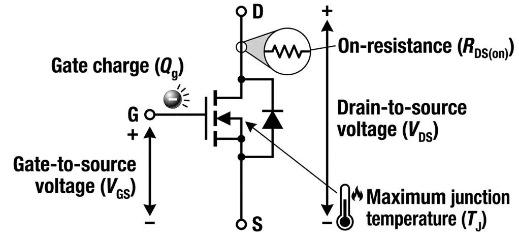
As shown in Fig-1, the key parameters that can impact the performance of MOSFETs are:
- Drain-source voltage (Vds)
- Gate-source voltage (Vgs)
- On-state resistance (Rds(on))
- Gate charge (Qg)
- Junction temperature (Tj)
Any of the aforementioned parameters exceeding safe operating conditions can lead to MOSFET failure.
Common Reasons for MOSFET Failure
Avalanche Breakdown (Voltage Overstress in MOSFETs)
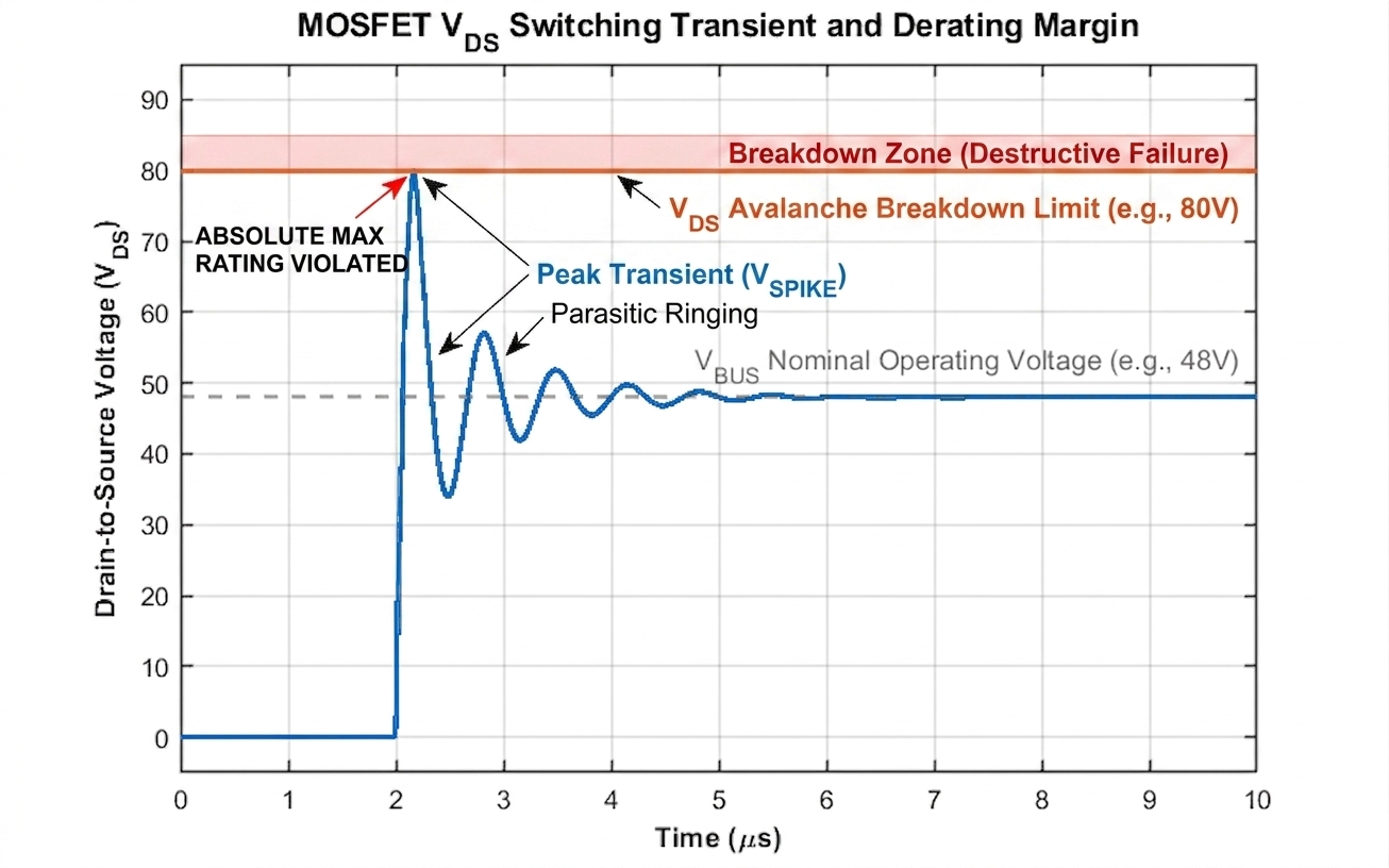
One of the most frequent causes of MOSFET failure is exceeding the maximum drain-source voltage (Vds) rating. This typically happens due to voltage spikes from parasitic inductances, poor snubber design, and inductive load switching.
Whenever current flows through an inductive path (motors, transformers, long PCB traces, etc.), the inductor resists the sudden change in the current. As soon as the MOSFET turns off, the stored energy in the inductor is released causing a high-voltage spike across the MOSFET terminals, as depicted in Fig-2. The energy stored in the inductor and voltage spike can be estimated using the following equations:
\[W =\frac{1}{2} L I^2\]
\[V =L\frac{di}{dt}\]
If the transient spike exceeds the Vds limit, the power semiconductor goes into avalanche breakdown. Although datasheets of some devices provide avalanche ratings (such as IRF540NPBF ), repeated stress results in gradual degradation and eventual failure.
Gate-Source Voltage (Vgs) Overstress
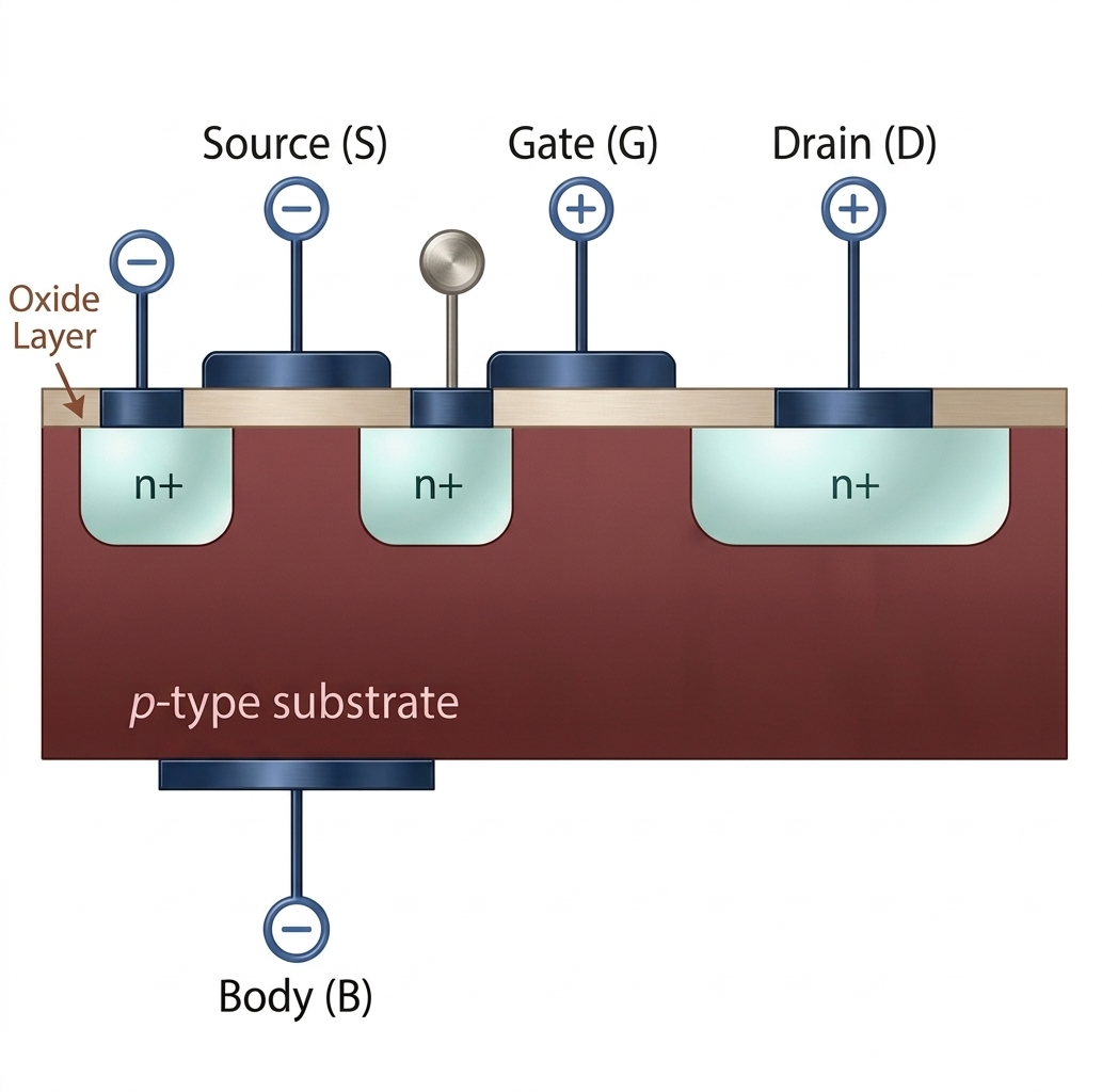
As demonstrated in Fig-3, the gate terminal of MOSFET is insulated from the other terminals by a fragile silicon dioxide layer. The absolute gate-source (Vgs) voltage for the most standard MOSFETs is generally in the range of ±20V (reference device: IPW60R075CPFKSA1). Exceeding these limits can permanently damage the oxide layer.
If a voltage (Vgs) higher than the rated voltage is applied to the gate terminal, the thin oxide layer breaks down, initiating a short circuit between gate and source terminals. This may damage MOSFET itself and associated gate driver circuit, potentially resulting in further system failure.
Higher Vgs often occurs due to transient effects such as ringing. Parasitic inductance available in gate drive loop, combined with input capacitance (Ciss) of MOSFET, establishes an unintended resonant circuit (LC). During the switching transitions, this resonance causes voltage spikes at the gate terminal.

Excessive Current and Thermal Overload in MOSFET
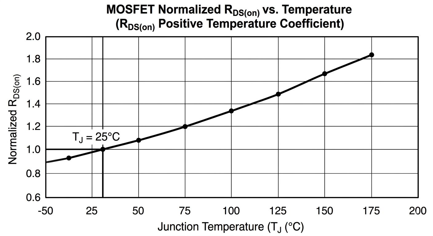
A MOSFET does not behave as an ideal switch; it has On-state resistance (Rds(on)). When the MOSFET is on, current flows through this resistance, leading to heat generation due to conduction losses. The conduction losses heavily depend on Rds(on) (low RDS(on) example: BSC026N08NS5ATMA1) and can be calculated as:
\[P = I^2R\]
In most standard MOSFETs, Rds(on) has a positive coefficient of temperature. As the temperature increases, the Rds(on) increases as shown in Fig-4. This behaviour can cause thermal runaway, ultimately resulting in device failure.
In addition, undersized MOSFET selection, poor PCB thermal design, and insufficient heat sinking can be potential reasons for MOSFET failure.
Gate Driver Issues
Inadequate selection of gate driver is one of the major causes for MOSFET failure. The gate of MOSFET must be supplied with correct voltage and timing to ensure efficient switching. For instance, driving a MOSFET with just 5V, when it requires 12V leads to excessive losses and overheating. Additionally, choice of improper gate resistance either slows down switching or cause ringing.
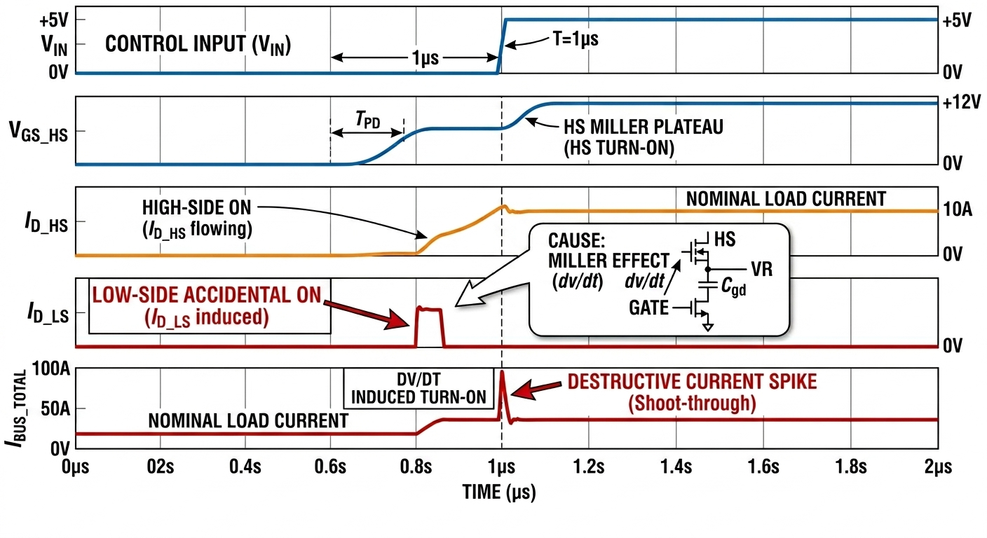
Miller Effect in MOSFET (dv/dt issues)
A MOSFET has an internal parasitic capacitance between its gate to drain terminals, also known as Miller capacitance (Cgd). In a half bridge configuration, when high side MOSFET turns-on, lower-side MOSFET experiences a sharp rise in Vds.
This high dv/dt causes a displacement current into the gate of lower-side MOSFET through the Miller capacitance (Cgd). If gate is not properly clamped, this induced current can raise the gate voltage beyond the threshold voltage (Vth) limit leading to short circuit.
As shown in Fig-5, this condition, generally referred to as shoot-through results in extreme current flowing through both devices instantaneously, leading to excessive power dissipation and ultimately MOSFET failure.
Poor PCB Layouts and Parasitics
PCB layout is as important as internal characteristics of the device. Poor PCB layout may introduce parasitic resistance and inductance, which can significantly impact the switching behaviour of MOSFET.
The most common layout mistakes include long traces, poor grounding, and large loop areas. This leads to increased inductances, voltage overshoot, and severe EMI issues. Especially, in high-speed switching circuits, even a small amount of parasitic inductance can introduce significantly large voltage spikes, surpassing the maximum Vds limit, consequently, causing a device failure.
Electrostatic Discharge (ESD)
Due to thin gate oxide layer, MOSFETs are highly sensitive to electrostatic discharge (ESD). Such that a small static charge can cause breakdown of gate oxide. Although, this type of damage may not cause an immediate failure, however, it can reduce reliability of the device over time.
MOSFET’s Body Diode Stress
During the operation in power converters, internal diode of MOSFET conducts current during particular operating conditions. Although, this is useful, it also introduces additional stress on the device.
These issues arise when reverse recovery is low and higher current flows through the diode. These large current spikes lead to increased switching losses and heat generation, degrading the device performance over time.
How to Prevent MOSFET Failures
Before selecting a MOSFET for power electronics design, several design checks and preventive measures are taken. Selection based on datasheet parameters alone is not sufficient, as reliability also depends on gate driver quality, thermal design, etc.
The previous sections discussed most common reasons for MOSFET failure, this section focuses on proper steps designers/engineers can adopt to avoid those failures.
How to Prevent MOSFET Failures: Avalanche Breakdown
- Proper device selection: Keep the safety margin for different parameters; Vds (>1.5-2×operating voltage), Ids (2-3 times), and Rds(on) (lower) (read our article on MOSFET selection guide).
- Snubber circuits: Place an RC snubber across the drain-source terminals. It damps the ringing and absorbs the energy of inductive spikes.
- PCB layout optimization: Every millimeter of trace adds parasitic inductance and creates high current spikes. Therefore, designers should minimize the loop area of high-current switching paths.
How to Prevent MOSFET Failures: MOSFET (Vgs) Overstress
- Gate resistor: Add a small series gate resistor (Rg), generally in between 1Ω-10Ω reduces ringing.
- Driver placement: Place the driver IC as close as possible to the MOSFET. This reduces loop inductance and improves switching performance.
- Zener diode: When working with critical and noisy load, place a Zener diode across the gate-source pins. It helps in clamping transient spikes form the inductive path.
How to Prevent MOSFET Failures: Excessive Current and Thermal Overload
- Current derating: Designers should derate current rating of MOSFET according to maximum junction temperature limits.
- Heat sinks: Use proper heat sinks to dissipate the heat from the system.
- Junction temperature calculations: Ensure that:
\[T_j = T_a + (P_d \times R_{\theta JA})\]
remains in safe operating limits.
How to Prevent MOSFET Failures: Gate Driver Issues
- Driver selection: Each system requires different drivers, hence designers should verify peak gate current, gate supply voltage, gate charge, etc. before selecting a gate driver IC.
How to Prevent MOSFET Failures: Miller Effect
- Asymmetric gate resistors: Use a diode in parallel with gate resistor. This helps in reducing the switching speed during turn-on (maintaining the faster speed during turn-off) resulting in low EMI and ringing issues.
- Active Miller clamping: Adopt advanced gate driver ICs with active Miller clamp features. These advanced drivers are capable of shorting the gate to ground, if unwanted voltage rise is observed.
How to Prevent MOSFET Failures: Testing Before Deployment
Circuit testing is one of the very essential steps to avoid MOSFET failure. Before deploying a circuit, engineers should test it under real operating conditions. Load variations, switching transients, ambient temperature, and fault conditions can expose weakness in a circuit that may not be visible during basic bench testing.
Use Instruments such as oscilloscope, thermal cameras to verify the performance of the system. This early-stage testing helps in identifying potential issues before the product reaches production stage.
Common Design Mistakes and Best Practices to Avoid MOSFET Failure
Device characteristics are not the sole cause of MOSFET failure. There are several design mistakes made by engineers such as, thermal management, gate driving, poor PCB layout, etc. The table below demonstrates the common mistakes made by engineers and recommended practices to improve reliability and long-term performance.
| Design Mistake | Recommended Practice |
| MOSFET selection without safety margin | The breakdown voltage of MOSFET must be higher than 1.5-2 times operating voltage (example: IPB65R190CFDAATMA1 is good for 400V systems ) |
| Avoiding current derating with temperature | Calculate power losses (conduction and switching losses) and identify the system maximum junction temperature |
| Using improper gate voltage (Vgs) | Select the suitable driver IC to ensure proper Vgs, peak gate current, etc. |
| Poor PCB layout | Minimise the power loops to reduce parasitic inductances in the design |
| Ignoring Safe Operating Area (SOA) limits | Review datasheet ratings, thermal derating and SOA limits |
| Weak grounding and noisy return path | Utilize proper grounding techniques to avoid noise issues. |
Conclusions
There are several reasons for MOSFET failures in the power circuits. In real-world applications, these failures occur due to incorrect component selection, poor PCB layout and thermal management, violating SOA limits, etc.
By examining different failure mechanisms such as overheating, switching transients, and parasitic inductances, engineers can significantly improve system reliability and overall performance. As discussed in this article, adopting preventive measures can eliminate many common problems in the power circuit.
Finally, a well-designed power circuit provides higher efficiency, robustness and improved system efficiency in power conversion, automotive and industrial applications.
Frequently Asked Questions (FAQs)
One of the most common reasons for MOSFET failure is operating the MOSFET beyond the breakdown voltage or drain current limit of the device. This often happens due to inductive spikes caused by inductive loads, long PCB traces, etc.
MOSFET thermal runaway is a catastrophic failure mode, where an increase in temperature causes higher current flow generating more heat, creating an uncontrollable cycle.
MOSFET heats up during the operation, its Rds(on) increases (positive temperature coefficient) as well. This higher resistance increases the conduction losses causing a component to dissipate more heat. If cooling system is not sufficient, the device temperature can surpass the maximum junction temperature limit leading to device failure.
Lifetime of MOSFET can be extended by using proper gate drive circuitry, limiting voltage overshoot, and reducing thermal stress by ensuring suitable cooling. In addition, operating a device below maximum ratings and following the SOA limits helps.
Shoot-through refers to two MOSFETs in a single leg turns on at the same time, creating a short circuit across the supply. This normally happens in a half bridge or full bridge topology. This results in massive amount of current flowing through MOSFETs and can destroy the device instantly.
To avoid shoot-through, engineers ensure a proper gate drive circuitry and dead time control.

COMMENTS